Roth & Rau - Ortner reveals FOUP purge system

The FOUP purge system reduces contamination and oxygen levels and improves yields in advanced semiconductor manufacturing processes
Roth & Rau - Ortner has introduced the FOUP Purge System that protects wafers from Airborne Molecular Contamination (AMC) and other chemical reactions, helping to improve yields and reduce costs.
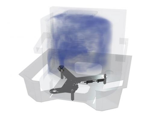
The purging system, pictured above, is especially aimed at semiconductor manufacturing process nodes of 28nm and below where minor contaminants can add excess time and costs to the development cycle.
The company unveiled the new system at SEMICON West 2014, where it is conducting live demonstrations of the FOUP Purge System at the booth of Silicon Saxony and the Saxony Economic Development Corporation in South Hall, booth #1829.
FOUP (Front Opening Unified Pod) is a specialised enclosure designed to hold silicon wafers in a controlled environment between process steps. The FOUP Purge System floods the FOUP with a constant flow of nitrogen during the interim storage period, flushing out harmful contaminants that can damage wafer surfaces.
Purging is a critical step and traditionally required a separate tool in the fab. Since the FOUP Purge System can be easily retrofitted to existing storage modules, the purging process no longer needs a separate station, resulting in cost savings and a zero footprint in the fab.
"At 28nm process nodes and below there is a dire need for protecting sensitive wafer surfaces against oxidation and other unwanted chemical reactions. With these ultra submicron geometries, humidity, ambient oxygen and even the slightest emission of molecules can cause surface defects, yield loss and other detrimental consequences," says Ulrich Spannring, head of sales for Roth & Rau - Ortner.
"Our FOUP Purge System is unique in that it provides permanent contamination protection via a constant flushing of the system during the entire time the wafers are stored, significantly reducing chances for surface contamination to cause problems. Also, since it can be easily retrofitted with existing FOUP storage systems, installation can be done during regular operations and no change is required to the fab structure or additional space needed."


