
Closing the gap in silicon nanowires
How do you put a puzzle together when the pieces are too tiny to pick up? Shrink the distance between them. Now scientists have shrunk the gap between nanowires to form dense arrays, making them useful for electronic devices
Engineers at the University of Illinois at Urbana-Champaign are using 'Shrinky Dinks', plastic that shrinks under high heat, to close the gap between nanowires in an array to make them useful for high-performance electronics applications. The group published its technique in the journal Nano Letters.
Nanowires are extremely fast, efficient semiconductors, but to be useful for electronics applications, they need to be packed together in dense arrays. Researchers have struggled to find a way to put large numbers of nanowires together so that they are aligned in the same direction and only one layer thick.
"Chemists have already done a brilliant job in making nanowires exhibit very high performance. We just don't have a way to put them into a material that we can handle," notes study leader SungWoo Nam, a professor of mechanical science and engineering at the U. of I. "With the shrinking approach, people can make nanowires and nanotubes using any method they like and use the shrinking action to compact them into a higher density."

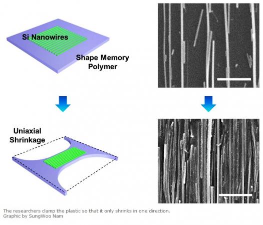
Shrinky Dinks plastic that shrinks when heated to pack nanowires together for electronics applications (Photo by SungWoo Nam)
The researchers place the nanowires on the Shrinky Dinks plastic as they would for any other substrate, but then shrink it to bring the wires much closer together. This allows them to create very dense arrays of silicon nanowires in a simple, flexible and very controllable way. This is illustrated in the image at the top of this story.
The shrinking method has the added bonus of bringing the nanowires into alignment as they increase in density. Nam's group demonstrated how even wires more than 30 degrees off-kilter can be brought into perfect alignment with their neighbours after shrinking.
"There's assembly happening at the same time as the density increases," Nam says, "so even if the wires are assembled in a disoriented direction we can still use this approach."
The plastic is clamped before baking so that it only shrinks in one direction, so that the wires pack together but do not buckle. Clamping in different places could direct the arrays into interesting formations, according to Nam. The researchers also can control how densely the wires pack by varying the length of time the plastic is heated. They also are exploring using lasers to precisely shrink the plastic in specific patterns.
Nam first had the idea for using Shrinky Dinks plastic to assemble nanomaterials after seeing a microfluidics device that used channels made of shrinking plastic. He realised that the high degree of shrinking and the low cost of plastic could have a huge impact on nanowire assembly and processing for applications.
"I'm interested in this concept of synthesising new materials that are assembled from nanoscale building blocks," Nam comments. "You can create new functions. For example, experiments have shown that film made of packed nanowires has properties that differ quite a bit from a crystal thin film."
One application the group is now exploring is a thin film solar cell, made of densely packed nanowires, that could harvest energy from light much more efficiently than traditional thin-film solar cells.
This research is described in detail in the paper, "Assembly and Densification of Nanowire Arrays via Shrinkage," by Jaehoon Bang et al in Nano Letters, 2014, 14 (6), pp 3304 - 3308. DOI: 10.1021/nl500709p


