+44 (0)24 7671 8970
More publications     •     Advertise with us     •     Contact us
 
News Article

Jordan Valley's wafer level packaging market share boosted

News

Jordan Valley Semiconductors, a supplier of X-ray based metrology tools for advanced semiconductor manufacturing lines, has announced that its micro-spot X-ray Fluorescence (µXRF) metrology tool has been qualified for production monitoring of advanced Wafer Level Packaging (WLP) processes, by another leading memory player.

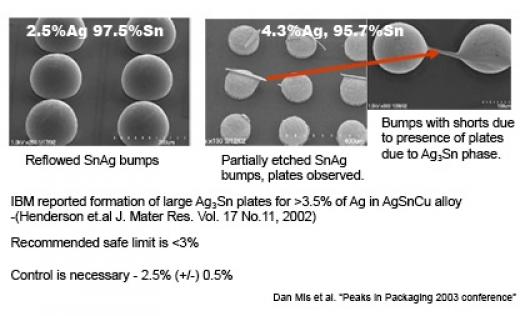
The tool provides fully automated metrology solutions for several key applications, including single µ-bump chemical composition and height measurements, as well as control of multi-layer Under Bump Metallisation (UBM) stack deposition.

Isaac Mazor, Jordan Valley's CEO, says, "We are glad to add another leading memory customer to our distinguished list of advanced customers. This is additional proof that Jordan Valley's tool and technology superiority is well appreciated and serves leading companies in the industry. Advancements in WLP technologies, such as the scaling down of solder bumps, complex UBM stacks, etc., set new metrology challenges and requirements that Jordan Valley can address. We believe that our tools will further contribute to our customer's high yield targets in the current and future WLP process."

Jordan Valley's micro-XRF metrology tool is suited to single bump composition measurements. It is ideal for non-destructive, in-line µ-bump % Ag measurements and uses a vertical excitation geometry that provides the smallest beam footprint with no dependence on height variation. The tool provides information critical for WLP process control, and comes with fully automated recipe driven measurements and analysis capabilities, advanced navigation algorithms for measurement on product wafers and more.

Jordan Valley's management will attend Semicon West 2014 in San Francisco from July 7th to 10th, 2014.


Purdue, imec, Indiana announce partnership
Resilinc partners with SEMI on supply chain resilience
NIO and NXP collaborate on 4D imaging radar deployment
Panasonic Industry digitally transforms with Blue Yonder
Global semiconductor sales decrease 8.7%
MIT engineers “grow” atomically thin transistors on top of computer chips
Keysight joins TSMC Open Innovation Platform 3DFabric Alliance
Leti Innovation Days to explore microelectronics’ transformational role
Quantum expansion
indie launches 'breakthrough' 120 GHz radar transceiver
Wafer fab equipment - facing uncertain times?
Renesas expands focus on India
Neuralink selects Takano Wafer Particle Measurement System
Micron reveals committee members
Avoiding unscheduled downtime in with Preventive Vacuum Service
NFC chip market size to surpass US$ 7.6 billion
Fujifilm breaks ground on new €30 million European expansion
Fraunhofer IIS/EAS selects Achronix embedded FPGAs
Siemens announces certifications for TSMC’s latest processes
EU Chips Act triggers further €7.4bn investment
ASE recognised for excellence by Texas Instruments
Atomera signs license agreement with STMicroelectronics
Gartner forecasts worldwide semiconductor revenue to decline 11% in 2023
CHIPS for America outlines vision for the National Semiconductor Technology Center
TSMC showcases new technology developments
Alphawave Semi showcases 3nm connectivity solutions
Greene Tweed to open new facility in Korea
Infineon enables next-generation automotive E/E architectures
Global AFM market to reach $861.5 million
Cepton expands proprietary chipset
Semtech adds two industry veterans to board of directors
Specialty gas expansion
×
Search the news archive

To close this popup you can press escape or click the close icon.
Logo
×
Logo
×
Register - Step 1

You may choose to subscribe to the Silicon Semiconductor Magazine, the Silicon Semiconductor Newsletter, or both. You may also request additional information if required, before submitting your application.


Please subscribe me to:


You chose the industry type of "Other"

Please enter the industry that you work in: