
Superconducting silicon qubits for quantum devices
Using a bottom-up approach, researchers have made hybrid quantum devices using silicon
Theorists have proposed a way to make superconducting quantum devices such as Josephson junctions and qubits, atom-by-atom, inside a silicon crystal. Such systems could combine the most promising aspects of silicon spin qubits with the flexibility of superconducting circuits. The researcher's results have now been published in Nature Communications.
High quality silicon is one of the historical foundations of modern computing. But it is also promising for quantum information technology. In particular, electron and nuclear spins in pure silicon crystals have been measured to have excellent properties as long-lived qubits, the equivalent of bits in conventional computers.
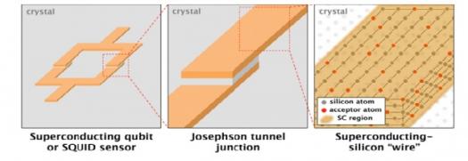
Examples of superconducting-silicon quantum devices are shown above. On the left is a superconducting loop interrupted at two points by junctions can form a superconducting flux qubit or a superconducting quantum interference device, or SQUID.Currents flowing in the loop can be used to measure the strength of a magnetic field threading the loop.
Yun-Pil Shim and Charles Tahan from the University of Maryland and the Laboratory for Physical Sciences have shown how superconducting qubits and devices can be constructed out of silicon. The Laboratory for Physical Sciences is affiliated with the Joint Quantum Institute (JQI).
Doing so can potentially combine the good quantum properties of silicon and the ubiquity of semiconductor technology with the flexibility of superconducting devices. They propose using "bottom-up" nano-fabrication techniques to construct precisely placed superconducting regions within silicon or germanium and show that such "wires" can be used to make superconducting tunnel junctions and other useful superconducting devices.
QUBITS IN SUPERCONDUCTORS AND SEMICONDUCTORSSuperconducting circuits, made from superconducting metals and Josephson tunnel junctions (which allow superconducting electron pairs to tunnel between two superconductors), are exceptionally customisable and can produce devices ranging from magnetic field sensors to classical logic circuits. They are also likely to play a big role in processing quantum information, where they can be used as a platform for qubits, tiny quantum systems which reside in a superposition of quantum states.
Several types of superconducting circuits have been used to implement qubits and quantum logic gates with different properties and potential uses. For example, in one kind of circuit current can flow in either of two directions.
These alternatives constitute the two superposed states needed for establishing a qubit. The two states can be labeled "0" and "1" in analogy with classical bits. Microwave pulses can drive transitions between the two levels allowing for quantum logic gates.
In general, quantum systems are delicate objects and are susceptible to noise and other environmental factors which diminish performance. Prospective quantum circuits must preserve qubits from outside interference for as long as the quantum calculation proceeds. Despite rapid progress in the quality of superconducting qubits (qubit lifetimes can now surpass 100 microseconds), qubit gate error rates are still limited by loss in the metals, insulators, substrates, and interfaces that make up the heterogeneous superconducting devices.
Spin qubits, are an example of qubits realized in a solid-state, silicon context. Spin is a quantum property of particles like an electron; physicists often think of an electron's spin as being like a small magnet, which will naturally point along the direction of an applied magnetic field. Here the 0 and the 1 states correspond to the two possible orientations of the electron spin, either up or down.
Because spin is naturally decoupled from charge in some systems (meaning the information stored in the direction of the spin will not be ruined by moving the electron or by it being shaken by electric noise), spin qubits are thought to be promising candidates for a robust qubit design
What's more, the use of epitaxial semiconductor devices, and the ability to bury spin qubits deep inside a semiconductor medium, far away from noise at interfaces and surfaces, has resulted in qubits that live for seconds or even hours in some situations, much longer than superconducting qubits to date.
PRACTICAL DEVICESShim and Tahan propose to use the best features of superconductor and semiconductor qubits. They aim to make superconducting wires and junctions, from which qubits and sensors can be made, by placing (or "doping") acceptor atoms (such as boron or aluminium, elements which readily accept extra electrons) in silicon in precise regions within the crystal. They suggest that a recently developed technique from the silicon qubit community, "STM hydrogen lithography", can be used to do just that.
Pioneered by Michelle Simmons at the University of New South Wales, a scanning tunneling microscope (STM) tip is used to selectively remove hydrogen atoms on the surface of silicon (or germanium). Doping gas such as phosphine can then be introduced, allowing the selective placement of impurities down to a single atomic site. "If acceptor atoms can be placed at sufficient density over enough layers, then superconducting regions can be fabricated within the silicon and then encapsulated with crystalline silicon," says Dr. Shim.
In some STM efforts as many as one-in-four silicon atoms have been replaced in this manner. And generally the higher the dopant density, the higher the critical superconducting temperature will be.
Scientists first learned about 10 years ago that silicon can be made superconducting if doped to sufficient density with acceptor atoms such as boron. In recent years, the quality of such superconducting silicon systems has improved greatly, yielding material with superconducting critical temperatures approaching 1 Kelvin and still leaving the crystal in good condition (in other words, it's still silicon).
By calculating the properties of these superconducting-semiconductor regions, Shim and Tahan show that wires with sufficient critical temperature can be constructed practically with the bottom-up hydrogen lithography approach. They also show that Josephson tunnel junctions and weak links, the fundamental non-linearity from which superconducting circuits can be constructed, can also be made.
Finally they show that the previously-demonstrated superconducting qubit types (seen in metal samples) can be constructed in this silicon system as well and provide the geometric requirements needed for fabrication.
"There is ongoing effort to make the tunneling barrier epitaxial to improve its quality," says Charles Tahan, "but no previous work to make the whole device out of a single semiconductor crystal. As far as we know, this is the first proposal on the feasibility of SC silicon for Josephson junctions and qubits. I'm also excited about these systems' potential for other devices such as sensors and particle detectors."
Beyond the possibility of superconducting circuits built inside a homogeneous silicon crystal, engineered superconducting-semiconductor devices like these could be used to build other types of exotic quantum many-body systems, at the atomic scale, and even act as testbeds for our understanding of superconductivity itself.
This work is detailed in the paper, "Bottom-up superconducting and Josephson junction devices inside a group-IV semiconductor," Y.P. Shim, C. Tahan, Nature Communications, 5, 4225 (2014)


