+44 (0)24 7671 8970
More publications     •     Advertise with us     •     Contact us
 
News Article

High-precision positioning of wafers in inspection systems

News

The current standard wafer has a diameter of 8". The industry is moving towards manufacturing larger wafers.  Technologies for production processes such as stealth dicing, lithography, doping, implanting, planarization makes precise positioning of the bigger substrates a must. Thin film technology places great demands on the substrates and their structures.

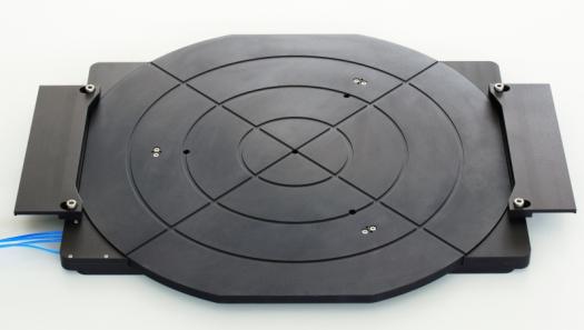
The piezosystem jena GmbH now offers a positioning system for the inspection of the new larger wafers. This system is designed to position wafers with a diameter up to 12" using precise hold and repeat positioning with the same precise precision. The system can be used as an automated inline controller or as a stand-alone positioner. The highly precise positioning system allows steady processes in production and process control. The new system will also shorten cycle times in quality control. Piezosystem jena's new system offers positioning in microseconds with steps of a few microns with repeatability in nanometers. Your crucial data will be obtained quickly with excellent performance and value.

Applications: 

"¢             semiconductor and solar producing

"¢             lithography

"¢             display production

"¢             surface structuring

"¢             Surface inspection

"¢             measurement chips

"¢             measurement of conductor tracks

"¢             measurement systems

"¢             quality control

"¢             bonding-technology

Purdue, imec, Indiana announce partnership
Resilinc partners with SEMI on supply chain resilience
NIO and NXP collaborate on 4D imaging radar deployment
Panasonic Industry digitally transforms with Blue Yonder
Global semiconductor sales decrease 8.7%
MIT engineers “grow” atomically thin transistors on top of computer chips
Keysight joins TSMC Open Innovation Platform 3DFabric Alliance
Leti Innovation Days to explore microelectronics’ transformational role
Quantum expansion
indie launches 'breakthrough' 120 GHz radar transceiver
Wafer fab equipment - facing uncertain times?
Renesas expands focus on India
Neuralink selects Takano Wafer Particle Measurement System
Micron reveals committee members
Avoiding unscheduled downtime in with Preventive Vacuum Service
NFC chip market size to surpass US$ 7.6 billion
Fujifilm breaks ground on new €30 million European expansion
Fraunhofer IIS/EAS selects Achronix embedded FPGAs
Siemens announces certifications for TSMC’s latest processes
EU Chips Act triggers further €7.4bn investment
ASE recognised for excellence by Texas Instruments
Atomera signs license agreement with STMicroelectronics
Gartner forecasts worldwide semiconductor revenue to decline 11% in 2023
CHIPS for America outlines vision for the National Semiconductor Technology Center
TSMC showcases new technology developments
Alphawave Semi showcases 3nm connectivity solutions
Greene Tweed to open new facility in Korea
Infineon enables next-generation automotive E/E architectures
Global AFM market to reach $861.5 million
Cepton expands proprietary chipset
Semtech adds two industry veterans to board of directors
Specialty gas expansion
×
Search the news archive

To close this popup you can press escape or click the close icon.
Logo
×
Logo
×
Register - Step 1

You may choose to subscribe to the Silicon Semiconductor Magazine, the Silicon Semiconductor Newsletter, or both. You may also request additional information if required, before submitting your application.


Please subscribe me to:


You chose the industry type of "Other"

Please enter the industry that you work in: