
MHI Launches Proprietary Room-temperature Wafer Bonding Machines
Mitsubishi Heavy Industries, Ltd. (MHI), has launched wafer bonding services performed using its wafer bonding machines, developed in-house, capable of bonding different kind of materials at room temperature.
Until now the company has offered trial services of this kind to businesses and other potential users considering the machine's adoption; now those same services have been expanded to include businesses and research institutes with no immediate plans to acquire the machine. In launching the new services, MHI aims to boost recognition of the effectiveness of room-temperature wafer bonding, a technology originating in Japan, as a means toward expanding machine sales; it also looks to develop bonding services into a new area of business.
Room-temperature bonding is a process whereby, by irradiating ion beams and atom beams in a vacuum, wafer surfaces become activated and bond. Because, unlike conventional bonding, no heating is necessary, room-temperature bonding can be applied to bond materials with different coefficients of thermal expansion; moreover, the technology is perfectly suited to the production of MEMS* devices, which demand superior finishing precision, and bio devices that cannot be heated. Bondable materials include silicons, oxide dielectrics, glass, compound semiconductors, metals, ceramics, etc.
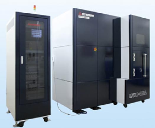
MHI completed development and commenced marketing of its first room-temperature wafer bonding machines in 2005. Today the lineup includes a fully automated system accommodating wafers up to 12 inches, or 300 millimeters (mm), which is capable of manufacturing three-dimensionally (3D) integrated LSI (large-scale integration) circuits. This newest system is rapidly coming into use in fields including MEMS sensors, light-emitting diodes (LED), high-frequency devices, biodevices, power devices, etc.
Until now, businesses and institutions planning to acquire MHI's room-temperature wafer bonding machine have confirmed the system's actual bonding performance and quality via bonding tests performed at MHI using actual material samples. In recent years, as the room-temperature bonding process itself has become a focus of interest around the world, MHI has seen a significant increase in such material bonding requests especially from university and business research laboratories and factories engaging in small-lot production. It was in light of these developments that MHI decided to accept requests for bonding services regardless of whether the user plans to acquire a machine or not.
The new bonding services are carried out using four demonstration systems located at the Technology & Innovation Headquarters' Advanced Technology Research Center in Yokohama and the Machine Tool Division in Ritto City (Shiga Prefecture). Fees vary depending on factors such as wafer size, number of units to be bonded, etc. Trial bonding of smaller-size chips is also performed under designated conditions.


