Element Six announce new thermal grade of CVD diamond

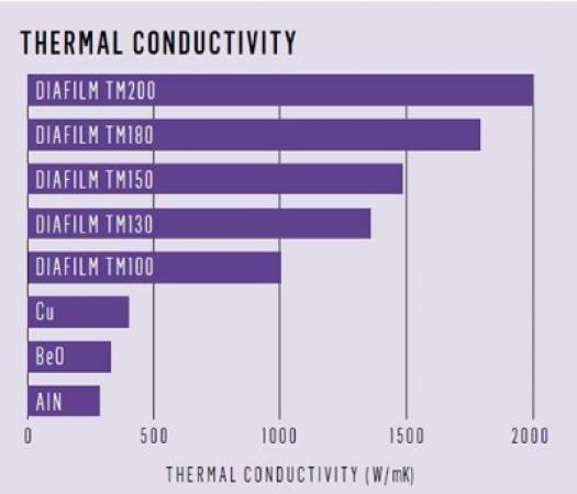
Element Six has announced the development of a new thermal grade of diamond grown by chemical vapour deposition (CVD), DIAFILM TM130. DIAFILM TM130 has a thermal conductivity in excess of 1300 W/mK and is available in both metallized and un-metallized wafers form. Similar to Element Six's material grades in its DIAFILM TM range, TM130 offers full isotropic heat spreading in both planar and through plane directions. Enhancing its already extensive portfolio to offer customers more options to address unique thermal management needs, Element Six now provides a total of five material grades spanning five levels of performance ranging from 1000 W/mK to 2000 W/mK.
"CVD diamond is the most thermally conductive material at room temperature, far surpassing the thermal conductivity of copper. With this new offering, we're continuing to build our extensive portfolio of thermal grade materials to meet the needs of those in the microelectronics and electronics packaging industry," said Director of Element Six Technologies, Adrian Wilson. "Recognizing a 'one-size fits all' approach is not effective, we're committed to providing a full range of options and specifications to effectively address thermal management challenges, including specific requirements for surface flatness, low roughness and metallization."
CVD diamond is uniquely suited for advanced thermal management in applications such as advanced packaging, due to its exceptional combination of properties including high thermal conductivity, mechanical strength, electrical insulation, low weight and chemical inertness. In this role, CVD diamond enables system size reductions, improved reliability and the opportunity to design higher power systems within an existing module footprint.
With a focus on customizability, Element Six's solid thermal products are available up to three millimeters thick and in diameters up to 140 millimeters that can be laser cut to any required size. Furthermore, metallization solutions enable die bonding with low thermal barrier resistance, consistent with industry standard soldering and brazing.
At the IMAPS 47th International Symposium on Microelectronics, Element Six will present on "Advanced Thermal Dissipation in GaN-on-Diamond Transistors," developed in conjunction with the University of Notre Dame, on Wednesday, Oct. 15 at 8 a.m. PT. This presentation will discuss the thermal barriers that stand in the way of achieving the intrinsic performance potential of gallium nitride (GaN) semiconductors. In reviewing challenges, the presentation will share details about a recent solution which replaces GaN's entire host substrate"”such as silicon (Si) or silicon carbide (SiC)"”with a synthetic diamond substrate, resulting in a more than 40 percent reduction of peak device temperature.


