
Advantest Launches System for Packaging Inspection
The TS9000 Mold Thickness Analysis (MTA) System is a new metrology tool that performs non-destructive analysis of the thickness of semiconductor packaging. Meeting the high standards of speed and accuracy required for high-volume manufacturing, its innovative inspection capabilities are expected to contribute significantly to product quality improvement amid the trends towards smaller device sizes and higher integration, driven in part by the widespread adoption of smartphones and tablets.
Already installed and in use, the TS9000 heralds a new product family of analysis systems for high-volume manufacturing. Future systems from the THz product family will target the pharmaceutical, automotive, ceramic and other industrial markets in addition to semiconductors. Advantest is leveraging its leading capabilities in terahertz technology to bring cutting-edge non-destructive analysis to industrial production lines.
The worldwide embrace of smartphones and other advanced consumer electronics is driving demand for smaller, more highly integrated semiconductor devices. Semiconductor packages for this market must be compact, thin, and tough enough to stand up to mobile usage. The semiconductor industry has few higher priorities than achieving an optimal balance of package durability and thinness.
However, existing metrology methods are not suitable for volume production lines. Manufacturers have had to test package thickness by inspecting samples late in the production process. Existing metrology methods are slow, laborious and destructive and not compatible with quality control in a high volume environment. This makes it difficult to assess the quality of the entire production run and problematic to trace the root cause of any defects in the final product.
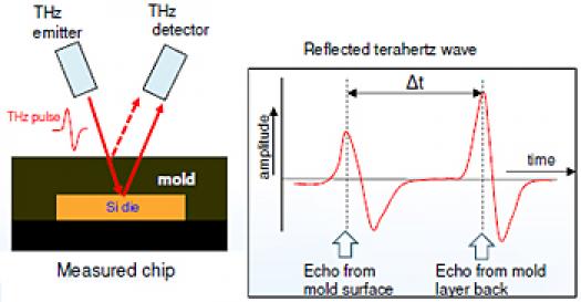
Advantest's TS9000 solves these issues by enabling rapid, repeatable, and highly accurate measurements of mold thickness, without the limitations of existing measurement methods. Highly adaptable, it can be deployed at various points in the assembly and packaging process, even immediately after the curing process, enabling earlier detection of production issues and improving product quality and yield.


