+44 (0)24 7671 8970
More publications     •     Advertise with us     •     Contact us
 
News Article

Plan Optik opens new 200 mm MEMS cap wafer line

News

Plan Optik AG has recently opened it's new 200 mm cap wafer fab in Germany.

The actual expansion of Plan Optik's capacity includes investments in latest grinding, CMP and anodic bonding equipment and not least automation of existing processes.

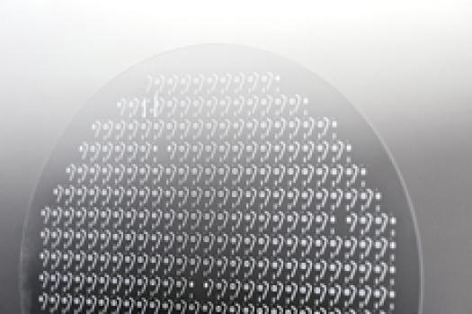
Plan Optik offers cap wafer solutions from glass and glass silicon compounds. This includes cap wafers for the packaging of optical MEMS such as CMOS image sensors, projection technology (DLP) and high power LED packaging.

Core processes used by Plan Optik are fully automatic grinding, polishing (CMP), (ultra sonic) drilling, sand blasting, wet etching and bonding glass and glass-silicon compound substrates. Materials used are borosilicate and alkaline free glass as well as silicon and silica (quartz).

Combining the big variety of processing techniques, Plan Optik offers cap wafers with optical (transparent) cavities, through holes for conductive connection as well as high accuracy blank glass substrates for best available performance. These wafers are clean room suitable and are already implemented in many high end sensor applications.

All wafers produced by Plan Optik are characterized by low ttv, thickness tolerance, low roughness and high surface quality. Plan Optik set the benchmark in respect to virtually perfect glass wafer surfaces by introducing it's proprietary development MDF polishing to the market. MDF (Micro Damaging Free) polished wafers are suitable for wet etching processes and avoid the well known issue sub surface damaging which can lead to defects. Sub surface damaging leads to small cavities and interconnections between the etched structures weakens the bonding interface and results in a low yield. The use of MDF polished wafers leads to reliable wet etching results and provides a high wafer processing yield.

Plan Optik, a public company located in Germany produces polished wafers for MEMS applications such as tire pressure monitoring systems and drug dispensing solutions since almost 20 years.

Plan Optik's ISO TS 16949, ISO 14001 and ISO 9001 certifications ensure the high quality all substrates are produced to.

Purdue, imec, Indiana announce partnership
Resilinc partners with SEMI on supply chain resilience
NIO and NXP collaborate on 4D imaging radar deployment
Panasonic Industry digitally transforms with Blue Yonder
Global semiconductor sales decrease 8.7%
MIT engineers “grow” atomically thin transistors on top of computer chips
Keysight joins TSMC Open Innovation Platform 3DFabric Alliance
Leti Innovation Days to explore microelectronics’ transformational role
Quantum expansion
indie launches 'breakthrough' 120 GHz radar transceiver
Wafer fab equipment - facing uncertain times?
Renesas expands focus on India
Neuralink selects Takano Wafer Particle Measurement System
Micron reveals committee members
Avoiding unscheduled downtime in with Preventive Vacuum Service
NFC chip market size to surpass US$ 7.6 billion
Fujifilm breaks ground on new €30 million European expansion
Fraunhofer IIS/EAS selects Achronix embedded FPGAs
Siemens announces certifications for TSMC’s latest processes
EU Chips Act triggers further €7.4bn investment
ASE recognised for excellence by Texas Instruments
Atomera signs license agreement with STMicroelectronics
Gartner forecasts worldwide semiconductor revenue to decline 11% in 2023
CHIPS for America outlines vision for the National Semiconductor Technology Center
TSMC showcases new technology developments
Alphawave Semi showcases 3nm connectivity solutions
Greene Tweed to open new facility in Korea
Infineon enables next-generation automotive E/E architectures
Global AFM market to reach $861.5 million
Cepton expands proprietary chipset
Semtech adds two industry veterans to board of directors
Specialty gas expansion
×
Search the news archive

To close this popup you can press escape or click the close icon.
Logo
×
Logo
×
Register - Step 1

You may choose to subscribe to the Silicon Semiconductor Magazine, the Silicon Semiconductor Newsletter, or both. You may also request additional information if required, before submitting your application.


Please subscribe me to:


You chose the industry type of "Other"

Please enter the industry that you work in: