
RIE An enabling technology for MEMS fabrication
Miniaturization of products is the flavour of the day. For the fast growing industries viz., semiconductor fabrication, instrumentation, space & aerospace, military and even in medical it is a continual process to be in the competitive technological world. Miniaturization of one part of a product often comes in uneven spurts of making other parts small of the overall design. So, the progresses of miniaturization of a specific technology leapfrog on other technologies.
Micromachining is the foundation of the technology to realize such miniaturized products. One of the recent and promising machining processes is a Reactive Ion Etching (RIE). It can be used as a machining process of Integrated Circuit (IC) devices, nano and micro scale devices. As such today, RIE is a key enabling technology for MEMS and NEMS fabrication.
Reactive Ion Etching (RIE) is a high resolution mechanism for etching materials. Samples are first masked by one of many patterning processes. They are then placed into a vacuum chamber. Gases are introduced into the chamber and then activated by RF or microwave power to create plasma. This plasma consists of a wide variety of reactive species, ions, and electrons. A negative DC bias is induced at the substrate by the free electrons. This bias accelerates ions in the plasma perpendicular to the sample surface. This provides a directional physical motivating force to etch.
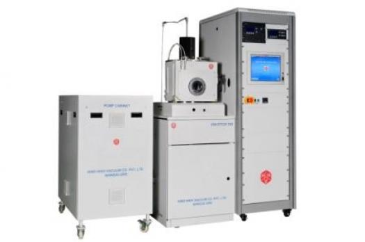
HHV's recent plasma system is designed for advanced etching applications. It is a standalone, manual/PC controlled Reactive Ion Etching (RIE) system. It is a versatile system with a shower head gas distribution of Argon (Ar), Oxygen (O2), SF6, CH3, CF4 and N2 gas distribution. It has a stain less circular chamber of size 300mm (diameter) x 300mm (ht) that open at the front for substrate loading. Chamber has view port for viewing the plasma. The round substrate holder can accommodate 2-6inch diameter substrate and the gap can be adjusted between substrate holder and the gas shower-head manually.
The chamber is extremely clean in design and reaches 10-9 mbar with the turbo-pump based pumping system. The RF power is provided by 600 W 13.5 MHz power supply. The system is completely automated and is PC controlled. A dry bed abatement system provided at the exhaust neutralizes the processed gases before it is out to atmosphere.


