
Breakthrough in flexible electronics enabled by inorganic-based laser lift-off
A research team led by Prof. Keon Jae Lee of KAIST provides an easier methodology to realize high performance flexible electronics by using the Inorganic-based Laser Lift-off (ILLO), which enables nanoscale processes for high density flexible devices and high temperature processes that were previously difficult to achieve on plastic substrates.
Flexible electronics have been touted as the next generation in electronics in various areas, ranging from consumer electronics to bio-integrated medical devices. In spite of their merits, insufficient performance of organic materials arising from inherent material properties and processing limitations in scalability have posed big challenges to developing all-in-one flexible electronics systems in which display, processor, memory, and energy devices are integrated. The high temperature processes, essential for high performance electronic devices, have severely restricted the development of flexible electronics because of the fundamental thermal instabilities of polymer materials.
A research team headed by Professor Keon Jae Lee of the Department of Materials Science and Engineering at KAIST provides an easier methodology to realize high performance flexible electronics by using the Inorganic-based Laser Lift-off (ILLO).
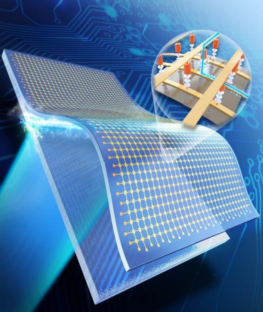
The ILLO process involves depositing a laser-reactive exfoliation layer on rigid substrates, and then fabricating ultrathin inorganic electronic devices, e.g., high density crossbar memristive memory on top of the exfoliation layer. By laser irradiation through the back of the substrate, only the ultrathin inorganic device layers are exfoliated from the substrate as a result of the reaction between laser and exfoliation layer, and then subsequently transferred onto any kind of receiver substrate such as plastic, paper, and even fabric.
This ILLO process can enable not only nanoscale processes for high density flexible devices but also the high temperature process that was previously difficult to achieve on plastic substrates. The transferred device successfully demonstrates fully-functional random access memory operation on flexible substrates even under severe bending.
Professor Lee said, "By selecting an optimized set of inorganic exfoliation layer and substrate, a nanoscale process at a high temperature of over 1000 °C can be utilized for high performance flexible electronics. The ILLO process can be applied to diverse flexible electronics, such as driving circuits for displays and inorganic-based energy devices such as battery, solar cell, and self-powered devices that require high temperature processes."


