
TSV based memory going to volume production
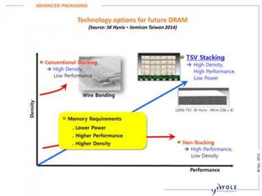
The challenges for DRAM are to reduce power consumption, satisfy required bandwidth and satisfy density (miniaturization) requirements all the while maintaining low cost. Applications are evolving with different demands on these basic requirements. For example graphics in a smartphone may require bandwidth of 15GB/sec while a networking router may require 300GB/sec.
Memory is also known to be the biggest user of power in server farms, thus there is a requirement in both portable devices and networking and server applications for low power memory solutions.
With the recent Samsung announcement of mass production of 64 GB DDR4 DIMMs that use TSV technology for enterprise servers and cloud-based applications, all three of the major DRAM memory manufactures, Samsung, Hynix and Micron, have now announced the commercialization of TSV based memory architectures.
Hynix has announced the release of multiple memory solutions over the next 2 years.
Emerging DRAM technologies such as wide IO, HMC and HBM are being optimized for different applications and present different approaches to address bandwidth, power, and area challenges. The common element to HMC, HBM and Wide IO are 3D technologies, i.e.
Wide I/O 2: supporting 3D-IC packaging for PC and server applications
Wide I/O increases the bandwidth between memory and its driver IC logic by increasing the IO data bus between the two circuits. Wide I/O typically uses TSVs, interposers and 3D stacking technologies.
The 2014 Wide I/O 2 standard JESD229-2 from JEDEC, is designed for high-end mobile applications that require high bandwidth at the lowest possible power. Wide I/O 2 provides up to 68GBps bandwidth, at lower power consumption (better bandwidth/Watt) with 1.1V supply voltage. From a packaging standpoint, the Wide I/O 2 is optimized to stack on top of a system on chip (SOC) to minimize power consumption and footprint. This standard trades a significantly larger I/O pin count for a lower operating frequency. Stacking reduces interconnect length and capacitance. The overall effect is to reduce I/O power while enabling higher bandwidth.
In the 2.5D-stacked configuration, cooling solutions can be placed on top of the two dies. With the 3D-stacked form of Wide I/O 2, heat dissipation can be an issue since there is no standard way to cool stacked die. The Hybrid Memory Cube is a specialized form of the wide I/O architecture.
The Hybrid Memory Cube (HMC) developed by Micron and IBM is expected to be in mass production in 2014. This architecture consists of 3D stacked DRAM layers on top of a controller logic layer. For example, 4 DRAM die are divided into 16 "cores" and then stacked. The logic base is at the bottom has 16 different logic segments, each controlling the four DRAMs cores that sit directly on top of it . This type of memory architecture supports a very large number of I/O pins between the logic and DRAM cores, which deliver bandwidths as high as 400GB/s. According to the Hybrid Memory Cube Consortium, a single HMC can deliver more than 15x the performance of a DDR3 module and consume 70 per cent less energy per bit than DDR3.
In addition to Micron and IBM, the HMC architecture developer members include Samsung, Hynix, ARM, Open Silicon, Altera, and Xilinx (HMC specs).
High bandwidth memory (HBM)
The 2013 JEDEC HBM memory standard, JESD235 was developed for high end graphics and gaming applications. HBM consisting of stacked DRAM die, built with Wide I/O and TSV, supports 128GB/s to 256GB/s bandwidths. TSMC has recently compared these different memory architectures in terms of bandwidth, power and price.
Architecture choice depends on application
Different applications will have different requirements in terms of bandwidth, power consumption, and footprint.
"¢ Because thermal characteristics are critical in high end smartphones, the industry consensus is that Wide I/O 2 is probably the best choice. Wide I/O 2 meets heat dissipation, power, bandwidth, and density requirements. However, it is more costly than LPDDR4.
"¢ Given its lower silicon cost, LPDDR4 is probably better suited for tablets and low end smart phones, less cost-sensitive mobile markets.
"¢ For high-end computer graphics processing, which are less constrained by cost then mobile devices, HBM memory may be the best choice.
"¢ High performance computing (HPC) or a networking router requiring 300GBps BW is probably best matched to the HMC.
The properties of these standardized memory architectures and the applications they appear best suited for are compared below.
As we move into 2015 several industry segments have announced applications using the new memory stacks.
"¢ Intel recently announced that their Xenon Phi processor "Knights Landing" which will debut in 2015 will use 16GB of Micron HMC stacked DRAM on-package, providing up to 500GB/sec of memory bandwidth for high performance computing applications.
"¢ AMD and Nvidia have also announced the use of HBM in their next generation graphics modules like the Nvidia Pascal due out in 2016.


