+44 (0)24 7671 8970
More publications     •     Advertise with us     •     Contact us
 
News Article

Silver Nanoislands grown by Atomic Layer Deposition

News

The new ALD Real Time Monitor was presented at the NRW Nano-Conference (1st-2nd of December 2014). This important conference welcomed its guests to participate the dialogue about opportunities and challenges of nanotechnology.

Optimizing atomic layer deposition processes with SENTECHs newly launched ALD Real Time Monitor was introduced to the German nanotechnology society. This tool features in situ measurement with 40 ms time resolution and a user-friendly software integration into the SENTECH atomic layer deposition system.

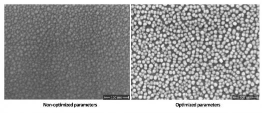
SENTECHs presentation focussed on monitoring silver nanoislands growth by plasma enhanced atomic layer deposition using SENTECH ALD. The growth of the silver islands was in situ monitored by the ALD Real Time Monitor, which allows thickness measurements with a sampling time of 40 ms. Dr Irina Kärkkänen, ALD specialist of SENTECH presented the results of the investigations by SENTECH ALD team. "High precision of the measurements and ultra-fast response of the ALD Real Time Monitor allow monitoring of single atomic layer deposition steps. Hence, the process is efficiently optimized in respect to precursor pulse, precursor purge, plasma pulse, and plasma purge. The optimized process parameters lead to silver nanoislands as confirmed by the SEM image." She concludes: "The ALD Real Time Monitor is a powerful system for in situ process monitoring."

The ALD Real Time Monitor is suited for optimized process development, e.g. silver nanoislands growth by plasma enhanced atomic layer deposition.

Purdue, imec, Indiana announce partnership
Resilinc partners with SEMI on supply chain resilience
NIO and NXP collaborate on 4D imaging radar deployment
Panasonic Industry digitally transforms with Blue Yonder
Global semiconductor sales decrease 8.7%
MIT engineers “grow” atomically thin transistors on top of computer chips
Keysight joins TSMC Open Innovation Platform 3DFabric Alliance
Leti Innovation Days to explore microelectronics’ transformational role
Quantum expansion
indie launches 'breakthrough' 120 GHz radar transceiver
Wafer fab equipment - facing uncertain times?
Renesas expands focus on India
Neuralink selects Takano Wafer Particle Measurement System
Micron reveals committee members
Avoiding unscheduled downtime in with Preventive Vacuum Service
NFC chip market size to surpass US$ 7.6 billion
Fujifilm breaks ground on new €30 million European expansion
Fraunhofer IIS/EAS selects Achronix embedded FPGAs
Siemens announces certifications for TSMC’s latest processes
EU Chips Act triggers further €7.4bn investment
ASE recognised for excellence by Texas Instruments
Atomera signs license agreement with STMicroelectronics
Gartner forecasts worldwide semiconductor revenue to decline 11% in 2023
CHIPS for America outlines vision for the National Semiconductor Technology Center
TSMC showcases new technology developments
Alphawave Semi showcases 3nm connectivity solutions
Greene Tweed to open new facility in Korea
Infineon enables next-generation automotive E/E architectures
Global AFM market to reach $861.5 million
Cepton expands proprietary chipset
Semtech adds two industry veterans to board of directors
Specialty gas expansion
×
Search the news archive

To close this popup you can press escape or click the close icon.
Logo
×
Logo
×
Register - Step 1

You may choose to subscribe to the Silicon Semiconductor Magazine, the Silicon Semiconductor Newsletter, or both. You may also request additional information if required, before submitting your application.


Please subscribe me to:


You chose the industry type of "Other"

Please enter the industry that you work in: