A new step towards using graphene in electronic applications

Few materials have received as much attention from the scientific world or have raised so many hopes with a view to their potential deployment in new applications as graphene has. This is largely due to its superlative properties: it is the thinnest material in existence, almost transparent, the strongest, the stiffest and at the same time the most strechable, the best thermal conductor, the one with the highest intrinsic charge carrier mobility, plus many more fascinating features. Specifically, its electronic properties can vary enormously through its confinement inside nanostructured systems, for example. That is why ribbons or rows of graphene with nanometric widths are emerging as tremendously interesting electronic components. On the other hand, due to the great variability of electronic properties upon minimal changes in the structure of these nanoribbons, exact control on an atomic level is an indispensable requirement to make the most of all their potential.
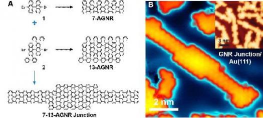
The lithographic techniques used in conventional nanotechnology do not yet have such resolution and precision. In the year 2010, however, a way was found to synthesise nanoribbons with atomic precision by means of the so-called molecular self-assembly. Molecules designed for this purpose are deposited onto a surface in such a way that they react with each other and give rise to perfectly specified graphene nanoribbons by means of a highly reproducible process and without any other external mediation than heating to the required temperature. In 2013 a team of scientists from the University of Berkeley and the Centre for Materials Physics (CFM), a mixed CSIC (Spanish National Research Council) and UPV/EHU (University of the Basque Country) centre, extended this very concept to new molecules that were forming wider graphene nanoribbons and therefore with new electronic properties. This same group has now managed to go a step further by creating, through this self-assembly, heterostructures that blend segments of graphene nanoribbons of two different widths.
The forming of heterostructures with different materials has been a concept widely used in electronic engineering and has enabled huge advances to be made in conventional electronics. "We have now managed for the first time to form heterostructures of graphene nanoribbons modulating their width on a molecular level with atomic precision. What is more, their subsequent characterisation by means of scanning tunnelling microscopy and spectroscopy, complemented with first principles theoretical calculations, has shown that it gives rise to a system with very interesting electronic properties which include, for example, the creation of what are known as quantum wells," pointed out the scientist Dimas de Oteyza, who has participated in this project.
This work, the results of which are published in the journal Nature Nanotechnology, therefore constitutes a significant success towards the desired deployment of graphene in commercial electronic applications.
Dr Dimas G. de Oteyza, who was previously at Berkeley and at the CFM, is currently working at the Donostia International Physics Center (DIPC) as a Fellow Gipuzkoa. The Fellows Gipuzkoa programme, funded by the Chartered Provincial Council of Gipuzkoa, is in fact devoted to bringing back young researchers with solid post-doctoral training in internationally prestigious groups and centres, by offering them a platform for reincorporation through contracts with a duration of up to five years, which enables them to compete in the best of conditions to obtain tenured positions as researchers in our country.


