
Thin Wafer Processing Temporary Bonding Adhesive Film For 3D Wafer Integration
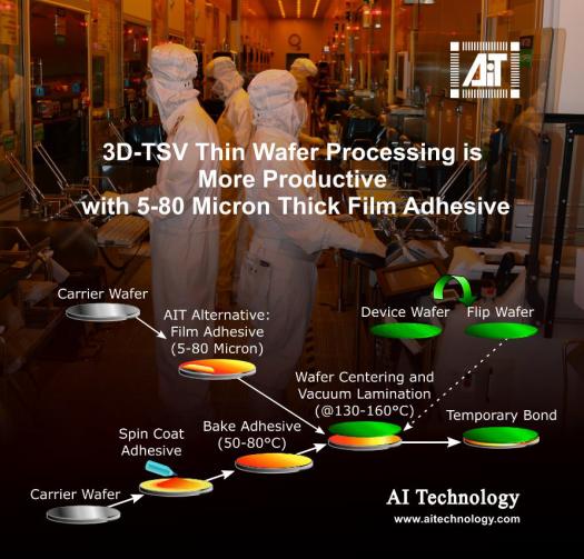
Temporary wafer bonding for thin wafer processing is one of the key technologies for wafer level 3D system integration. AI Technology, Inc (AIT) is proud to be the first known provider of a film format high temperature temporary bonding adhesive for thin wafer processing of bonding device wafer to carrier wafer. Leveraging its expertise manufacturing film adhesives for the semiconductor industry over the last 30 plus years, AIT offers Wafer Processing Adhesives (WPA) from 5 to 80 micron film adhesives for device wafer processing up to 450mm with and without topography. AIT high temperature capable WPA removes easily with laser assisted and solvent assisted release separation de-bonding besides traditional heat-sliding processes.
AI Technology, Inc. (AIT)'s temporary bonding Wafer Processing Adhesives (WPA) are thermally stable to 320-330°C and the bonded compound wafers are compatible with standard WLP process equipment and for backside processing of 3D-TSV wafers. High integrity in bond strength enables easy back grinding to a thickness of 50 μm. AIT's thermally and chemically stable polymers can withstand multiple device wafer processes, such as dry etching, wet etching, CMP, PVD, solvent based spin coating of resists and polymers, lithography, electro plating and extended elevated temperature processing up to 320-330°C for at least 60 minutes under high vacuum.
In comparison to traditional wax based and polyimide based temporary handling solutions, AI Technology, Inc. (AIT)'s WPA-TS 320 and WPA-TL 330 demonstrate some of the highest temperature capabilities for thin wafer processing as well as easy removal and cleaning.
Select Wafer Processing Applications:
TEMPORARY BONDING FOR WAFER THINNING AND PROCESSING OF THIN WAFERS
 Outstanding shear stress support for wet mechanical grinding and dry etching
 Unparalleled thermal stability for extended high temperature oxide deposition up to 320°C
TEMPORARY BONDING FOR THIN WAFER BUMPING AND ASSEMBLY OF THIN ICS
 Outstanding molecular stability with 0% weight loss for void free bonding at temperatures up to 330°C
 High temperature dimension stable stress-absorbing adhesive for solder bump reflow that can be separated or removed with solvent or laser assisted de-bonding
TEMPORARY BONDING FOR HIGH TOPOGRAPHY THIN WAFER PROCESSING
 Film adhesive of the same spin coating solution in any thickness, in addition to AI Technology, Inc. (AIT)'s standard 5, 10, 20, 40, 60 and 80 micron thicknesses
 Outstanding degree of planarization with vacuum lamination at a melt-flow temperature of approximately 150°C


