
Applied Materials Enables the Extension of Multiple Patterning to 10nm and Beyond
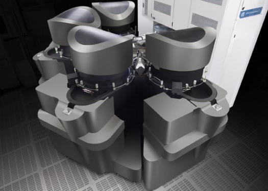
Applied Materials has announced the Applied Centura Tetra Z Photomask Etch system for etching next-generation optical lithographic photomasks needed by the industry to continue multiple patterning scaling to the 10nm node and beyond. The new tool extends the capabilities of Applied's industry-leading Tetra platform, delivering angstrom-level photomask accuracy for critical dimension (CD) parameters required to meet stringent patterning specifications for future logic and memory devices.
"Our Tetra Z system represents the state of the art in photomask etch technology, employing advances in precision materials engineering and plasma reaction kinetics to extend the use of 193nm lithography," said Rao Yalamanchili, general manager of Applied's Mask Etch product division. "Using the 193nm wavelength to produce 10nm or 7nm patterns requires a range of optimization techniques, including immersion and multiple patterning, which rely heavily on photomasks. Etch technology is key for photomask fabrication; the Tetra Z system is unique in delivering the accuracy required to etch next-generation optical photomasks for patterning advanced node designs."
Applied developed the Tetra Z tool for advanced chrome, MoSi*, hard mask and quartz (fused silica) etch applications used to fabricate advanced binary and phase-shift masks (PSMs). Offering continuous technical innovations and unprecedented CD performance, the system extends immersion lithography for quadruple patterning and cutting-edge resolution enhancement techniques. Vital capabilities ensuring pattern transfer fidelity include uniform, linear precision etching across all feature sizes and pattern densities with virtually zero defectivity.
Excellent CD performance combined with high etch selectivity enable the use of thinner resist films for achieving smaller photomask CD patterns on critical device layers. Controllable CD bias capability expands the system's flexibility to meet customer specific requirements. Unique quartz etch depth control ensures precision phase angle and aids integrated circuit scaling by providing customers the capability to use alternating aperture PSMs and chromeless phase lithography. These key advances derive from a variety of system improvements in chamber design, plasma stability, ion and radical control, flow and pressure control, and real-time process monitoring and control.
Applied's Tetra systems have been selected by a majority of mask makers worldwide to etch high-end photomasks over the past decade.


