
EV Group Sees Strong Demand For Emerging Photonic Applications
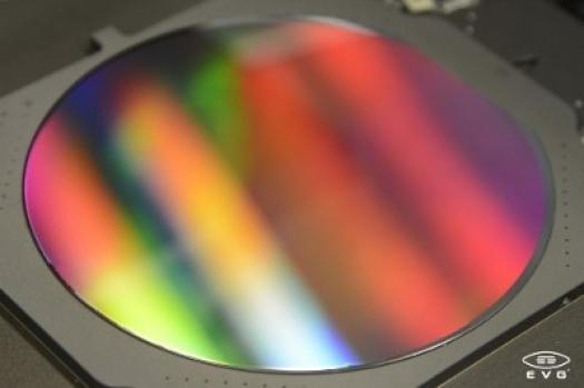
EV Group (EVG), a supplier of wafer bonding and lithography equipment for the MEMS, nanotechnology and semiconductor markets, today announced that its NILPhotonics Competence Center"”established to assist customers in enabling new and enhanced products and applications in the field of photonics"”has generated strong interest from customers and resulted in multiple system orders since its launch in December 2014. New system orders have included the company's EVG700/7000 Series UV-NIL (UV nanoimprint lithography) systems with SmartNIL technology to support high-volume manufacturing applications, including displays, light emitting diodes (LEDs) and wafer-level optics.
Since its initial launch, the NILPhotonics Competence Center has also expanded the products and applications it is supporting. These include photonic and microfluidic devices for bio-medical applications that pave the way for faster and more accurate diagnosis of diseases, as well as plasmonic structures that simultaneously carry optical and electrical signals and can be scaled to the smallest dimensions to enable new chip designs as well as better-performing devices, such as waveguides and sensors.
"The prevailing perception has been that despite the potential benefits of NIL technology, the barrier to entry for integrating it into high-volume manufacturing (HVM) is high. That simply isn't the case. EV Group has invested significant resources over many years in developing NIL technology as an HVM-capable solution for a number of applications," stated Markus Wimplinger, corporate technology development and IP director at EV Group. "Today, we have the world's largest installed base ofmore than 200 systems at customer facilities around the globe supporting volume-manufacturing of LEDs, MEMS, optics, photovoltaics and other devices. Our NILPhotonics Competence Center allows us to more easily bring all of our process and product capabilities and expertise to bear in helping our customers enable new photonic products and applications."
EVG's NILPhotonics Competence Center leverages EVG's field-proven process and equipment know-how in NIL and other process areas such as wafer bonding to support emerging photonic applications and significantly shorten time to market through fast process implementation and optimization, as well as through customized equipment design. In addition, EVG has a global partner network to draw from to support its customers' process integration and optimization efforts across the NIL infrastructure, including template manufacturing, resist materials and supporting equipment. As a result, EVG is able to provide consultation and support across all phases of the product lifecycle"”from design for manufacturing and prototyping through process development, qualification runs, pilot manufacturing and process transfer.
"More than a decade ago, EV Group launched the NILCom Consortium with support from companies representing key aspects of the NIL supply chain in order to speed commercialization of NIL technology. Through the dedicated efforts of all of our members, we are pleased to announce that the NILCom Consortium has successfully completed its charter and will end formal operations. That said, we will continue to collaborate with companies across the NIL supply chain including our former members as needed to ensure that NIL technology continues to address future customer roadmap requirements," added Wimplinger.


