
Scientists tune X-rays with tiny mirrors
Scientists at the U.S. Department of Energy's (DOE) Argonne National Laboratory have created a new way of manipulating high-intensity X-rays, which will allow researchers to select extremely brief but precise X-ray bursts for their experiments.
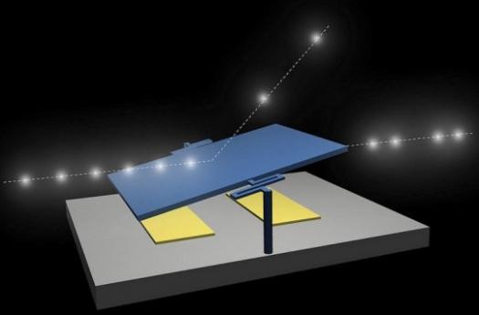
The new technology, developed by a team of scientists from Argonne's Center for Nanoscale Materials (CNM) and the Advanced Photon Source (APS), involves a small microelectromechanical system (MEMS) mirror only as wide as a few hairs.
MEMS are microscale devices fabricated using silicon wafers in facilities that make integrated circuits. The MEMS device acts as an ultrafast mirror reflecting X-rays at precise times and specific angles.
"Extremely compact devices such as this promise a revolution in our ability to manipulate photons coming from synchrotron light sources, not only providing an on-off switch enabling ultrahigh time-resolution studies, but ultimately promising new ways to steer, filter, and shape X-ray pulses as well," said Stephen Streiffer, Associate Laboratory Director for Photon Sciences and Director of the Advanced Photon Source. "This is a premier example of the innovation that results from collaboration between nanoscientists and X-ray scientists."
The device that the Argonne researchers developed essentially consists of a tiny diffracting mirror that oscillates at high speeds. As the mirror tilts rapidly back and forth, it creates an optical filter that selects only the X-ray pulses desired for the experiment. Only the light that is diffracted from the mirror goes on to hit the sample, and by adjusting the speed at which the MEMS mirror oscillates, researchers can control the timing of the X-ray pulses.
According to Argonne nanoscientist Daniel Lopez, one of the lead authors on the paper, the device works because of the relationship between the frequency of the mirror's oscillation and the timing of the positioning of the perfect angle for the incoming X-ray. "If you sit on a Ferris wheel holding a mirror, you will see flashes of light every time the wheel is at the perfect spot for sunlight to hit it. The speed of the Ferris wheel determines the frequency of the flashes you see," he said.
"The Argonne team's work is incredibly exciting because it creates a new class of devices for controlling X-rays," added Paul Evans, a professor of materials science at the University of Wisconsin-Madison. "They have found a way to significantly shrink the optics, which is great because smaller means faster, cheaper to make, and much more versatile."
In the future, the MEMS devices could split an X-ray pulse into even tinier, faster, and more precise slices by oscillating the device many millions of times a second, according to Argonne emeritus scientist Gopal Shenoy. "It will herald a new era of dramatically new and improved kinds of X-ray experiments," he said.
"The advantage of this new device is that it provides a very cheap way to generate and manipulate X-rays, and it can be adapted to virtually any X-ray facility in the world that already exists," Lopez said.
"The successful application of the MEMS technology to manipulate an X-ray beam at very high frequencies will certainly lead to further, more elaborate X-ray optical schemes for studying the structure and dynamics of matter at atomic length and time scales," added Edgar Weckert, the director of photon science at DESY, a German synchrotron research facility.
"This work is a very interesting first step of the MEMS application to X-ray optics. I am looking forward to the progression of the technology and its applications in wider fields at next-generation light sources," said Tetsuya Ishikawa, the director of the RIKEN SPring-8 Center in Japan. These include newly planned light source facilities such as the Advanced Photon Source Upgrade. "Such small sources and tiny MEMS devices form an ideal combination to make 3-D X-ray ultrafast movies with nanometer resolution," added Jin Wang, a senior scientist at the APS and one of the lead authors.
Journal Reference:
D. Mukhopadhyay, D. A. Walko, I. W. Jung, C. P. Schwartz, Jin Wang, D. López, G. K. Shenoy. X-ray photonic microsystems for the manipulation of synchrotron light. Nature Communications, 2015; 6: 7057 DOI: 10.1038/ncomms8057

Scientists at Argonne have created a new way of manipulating high-intensity X-rays, which will allow researchers to select extremely brief but precise X-ray bursts for their experiments. This schematic of their MEMS device consisting of a small oscillating mirror illustrates the reflection of an incoming X-ray at a particular critical angle.
Credit: Image courtesy Daniel Lopez


