
Rudolph Receives JetStep Lithography System Order from OSAT manufacturer
Rudolph Technologies, Inc has announced that a leading Taiwan-based outsourced assembly and test (OSAT) manufacturer has selected the JetStep W2300 Advanced Packaging Lithography System for the development of next-generation advanced packaging technology. The system will be used to enhance the wafer-level chip scale packaging (WLSCP) manufacturing process for both flip chip copper (Cu) pillar and fan-out wafer level packaging (FOWLP). Enhanced performance of these processes will help to further advance system-in-package (SiP) processes. The system is expected to ship in the third quarter and joins an extensive array of inspection and metrology systems to enhance Rudolph's footprint in the customers' advanced packaging facility.
"Achieving high-yield lithography for plating processes, such as copper pillar bumping and fan-out wafer level packaging, presents many challenges for manufacturers," stated Rich Rogoff, vice president and general manager of Rudolph's Lithography Systems Group. "They have been forced to purchase lithography tools customized for each process. The JetStep System has been demonstrated to achieve superior performance in both Cu pillar and FOWLP applications, allowing our customers to maintain a flexible factory by utilizing a single lithography solution that is able to produce a multitude of products in a highly cost-competitive manner.
"This commitment from yet another leading OSAT is further validation of the value of the JetStep System to accelerate advance packaging solutions," added Rogoff. "The superior applications performance coupled with unique wafer handling capabilities provides our customers with the best cost-of-ownership for advanced packaging lithography."
Mike Plisinski, Rudolph's executive vice president and chief operating officer, added, "We are very pleased with the customer response to the JetStep System. This order represents the third installation for the FOWLP process and the second installation for the Cu pillar process. This demonstrates a solid expansion of our customer base as well as growth in our application space over the last 12 months."
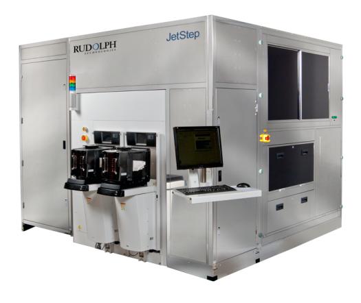
The JetStep Advanced Packaging Lithography product family has been specifically designed to provide solutions to address the challenges of newly-developed processes emerging in advanced packaging manufacturing. The JetStep W Series is intended for use with wafers or other round substrates. The JetStep S Series is for square or rectangular substrates. Both systems feature a 2X reduction stepper with a large field of view (52mm x 66mm) to improve exposure efficiency and throughput. The systems are unique in their ability to handle the wide range of substrates and to accommodate substrate warp, challenges that frequently encountered in the advanced packaging manufacturing processes. These and other purpose-designed features, such as on-the-fly auto focus and large automatic magnification compensation range, provide solutions that increase throughput and maximize yield in advanced package applications that are unavailable from legacy lithography tools initially designed for front-end, wafer-based processes.


