
Morgan Advanced Materials invests in the semiconductor market
Morgan Advanced Materials has made a further major investment in its capability for manufacturing semiconductor processing products, at its Technical Ceramics facility at Rugby in the UK.
The investment confirms Morgan's ongoing commitment to optimising its manufacturing capabilities in order to best serve its growing global customer base.
In particular, capital investment in new grinding equipment and an additional kiln has significantly increased Morgan's capacity. Semiconductor processing equipment is an area where Morgan has been performing particularly well recently and is seen as an area of growth for the company. As a result, Morgan is now better equipped to take on larger scale projects, supporting its ambitious growth objectives.
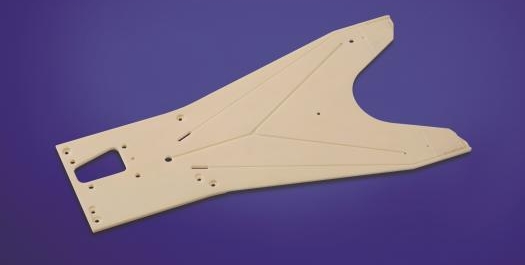
Through this investment, Morgan's Technical Ceramics business is now capable of precision grinding products of up to 500mm in diameter and 600mm in length, or longer lengths with smaller diameters, and manufacturing complex brazed assemblies incorporating its own metallisation inks.
The investment was made in response to increased demand for high purity alumina products from the semiconductor industry, but also from the medical and aerospace sectors. Products for the semiconductor industry include end effectors for efficient wafer handling, inductively-coupled plasma chambers / plasma focus tubes, ring spacers and electrostatic chucks (ESCs), which can be supplied either metallised or bare in diameters up to 450mm. Morgan's proven range of high purity materials are eminently suitable for use in high vacuum environments because they do not outgas.
With more than 60 years of experience in supplying premium custom ceramic components, Morgan has unrivalled experience of meeting the needs of the semiconductor industry. While it has the capability to create innovative engineered solutions for its customers on a batch and high-volume basis, it also has the expertise to competitively develop and produce high-quality prototypes to customer specifications, enabling semiconductor manufacturers to optimise their processes, maximise yields and reduce costs.

Phil Shakespeare, Engineering Manager, commented: "Our technical expertise and increased manufacturing capability enable us to deliver innovative, high-quality products to the market. We are the ideal choice for customers who need us to create bespoke solutions - our team of materials scientists and technical engineers have the know-how to work with customers to develop technical solutions for the most demanding applications."


