+44 (0)24 7671 8970
More publications     •     Advertise with us     •     Contact us
 
News Article

SUSS MicroTec Launches Semi-Automated High-Force Wafer Bonder

News

SUSS MicroTec, a supplier of equipment and applications for the semiconductor industry has launched the new bonding platform XB8. 

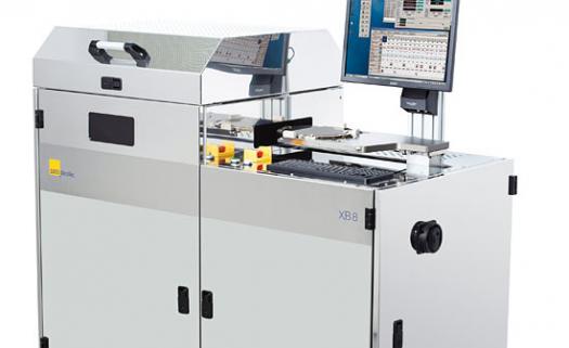
The XB8 wafer bonder is designed for a wide range of bonding processes. It supports substrates with a wafer size of up to 200 mm. Key process parameters can be adjusted in a wide range, which makes the system ideal for advanced process development. In a production environment, the high level of automation and reliability of the XB8 ensure a high level of process stability.

Typical applications include advanced packaging, MEMS, 3D integration and LED manufacturing. Suss say the XB8 wafer bonder offers a broad parameter window and is therefore suitable for carrying out all bonding processes. Bond force up to 100kN is available with a temperature range of up to 550°C. Different substrate shapes and wafer sizes are processed in specifically adapted fixtures. A multi-bond fixture, for example, enables the maximum possible throughput increase by bonding up to eight wafers at once.

"In addition to the high precision and the repeatability of the bonding process from wafer to wafer, a uniform process result across the wafer is essential for achieving a high yield.", says Stefan Lutter, General Manager of the bonder product lines. "The independent new heaters guarantee an even temperature distribution and also ensure an optimal bonding force homogeneity within the entire temperature range. The innovative mechanical and thermal structure of the XB8 wafer bonder enables optimal bonding force and temperature distribution across the wafer, resulting in a high product quality and yield."

Purdue, imec, Indiana announce partnership
Resilinc partners with SEMI on supply chain resilience
NIO and NXP collaborate on 4D imaging radar deployment
Panasonic Industry digitally transforms with Blue Yonder
Global semiconductor sales decrease 8.7%
MIT engineers “grow” atomically thin transistors on top of computer chips
Keysight joins TSMC Open Innovation Platform 3DFabric Alliance
Leti Innovation Days to explore microelectronics’ transformational role
Quantum expansion
indie launches 'breakthrough' 120 GHz radar transceiver
Wafer fab equipment - facing uncertain times?
Renesas expands focus on India
Neuralink selects Takano Wafer Particle Measurement System
Micron reveals committee members
Avoiding unscheduled downtime in with Preventive Vacuum Service
NFC chip market size to surpass US$ 7.6 billion
Fujifilm breaks ground on new €30 million European expansion
Fraunhofer IIS/EAS selects Achronix embedded FPGAs
Siemens announces certifications for TSMC’s latest processes
EU Chips Act triggers further €7.4bn investment
ASE recognised for excellence by Texas Instruments
Atomera signs license agreement with STMicroelectronics
Gartner forecasts worldwide semiconductor revenue to decline 11% in 2023
CHIPS for America outlines vision for the National Semiconductor Technology Center
TSMC showcases new technology developments
Alphawave Semi showcases 3nm connectivity solutions
Greene Tweed to open new facility in Korea
Infineon enables next-generation automotive E/E architectures
Global AFM market to reach $861.5 million
Cepton expands proprietary chipset
Semtech adds two industry veterans to board of directors
Specialty gas expansion
×
Search the news archive

To close this popup you can press escape or click the close icon.
Logo
×
Logo
×
Register - Step 1

You may choose to subscribe to the Silicon Semiconductor Magazine, the Silicon Semiconductor Newsletter, or both. You may also request additional information if required, before submitting your application.


Please subscribe me to:


You chose the industry type of "Other"

Please enter the industry that you work in: