Better smartphones? Nanosheets given local magnetic properties

Two-dimensional crystals are very suitable for creating high-quality magnetic thin films. Researchers show that by growing the magnetic layers on various 2D crystals, better known as nanosheets, you can control the preferred direction of the magnetism very locally. Scientists present this method to create magnetic patterns on the micrometer scale. They also demonstrate that you can make the nanosheets in less than a minute, while the synthesis process had been known to be very slow. The magnetic films can be deployed for many different applications, such as new generations of smartphones.
Two-dimensional crystals are very suitable for creating high-quality magnetic thin films. This appears from two recent publications written by scientists from the University of Twente's MESA+ research institute. The researchers show that by growing the magnetic layers on various 2D crystals, better known as nanosheets, you can control the preferred direction of the magnetism very locally. In an article published in Advanced Functional Materials, they present this method to create magnetic patterns on the micrometer scale. In Angewandte Chemie, they demonstrate that you can make the nanosheets in less than a minute, while the synthesis process had been known to be very slow. The magnetic films can be deployed for many different applications, such as new generations of smartphones.
With pulsed laser deposition (PLD) you can achieve controlled growth of thin layers of certain materials. Here, a material is heated rapidly with a powerful laser beam, so that it evaporates and a plasma is created. This spreads quickly in a vacuum chamber and is deposited on a substrate where it forms a thin layer. In this way you can control the thickness of the layer and you can form smooth and thin layers, often with special properties that are interesting for use in electronics and electro-mechanics, for example. For such applications, it is however essential that you can also make patterns in the layered materials. This is not easy, especially because the substrate needs to be heated to temperatures above 500° C during the PLD process. Many of the existing methods are therefore not adapted to existing manufacturing methods for microstructures.
Use of nanosheets
The UT researchers have now developed a new method, in which they make use of nanosheets obtained from three-dimensional crystals with a layered structure. If you dissolve these crystals in a special liquid, they spontaneously disintegrate into individual nanosheets. It was long thought that the crystal disintegration process could take weeks. However, the researchers have now shown that the nanosheets are already able to form within a few seconds, which opens the way for the production of nanosheets on a large scale.
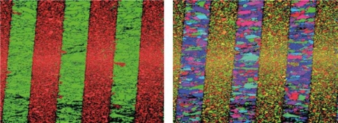
Based on the solution, various nanosheets can be introduced in micro-patterns on a substrate. These patterns form the starting point for the growth of thin magnetic layers of magnetic LaSrMnO3 at high temperatures by means of PLD. Depending on the type of nanosheet the structure of the magnetic film assumes a specific orientation, and thus determines the magnetism of the film at that location. The process is monitored by means of, for example, electron backscatter diffraction (EBSD); a technique that makes it possible to 'reveal' the structure in the patterns.
Functional properties
The researchers show that you can use the micro patterns to control the functional properties of a material in detail. In addition to magnetism, it is possible to pattern other properties at the micrometer scale. An important step has thus been taking in bridging the gap between scientific research into artificial layered crystals and their ultimate application.


