
AML Aligned Wafer Bonding
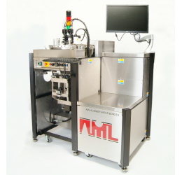
AML manufactures unique in-situ aligned wafer bonding machines and provides services based around waferbonding in its state-of-the-art multi-million pound Bondcentre facility situated on UK's premiere science park in Harwell, Oxfordshire.
Main benefits of AML Aligned Wafer Bonding
The design of the AML-AWB benefits from over 20 years' experience of Aligned - Wafer Bonding at AML.
Align & Bond
No wafer movement between alignment & bonding "“ guaranteed alignment accuracy
Simultaneous alignment, heating and vac pump-down (fastest cycle time)
In-bond chamber alignment at bond temperature (reduces expansion misalignment effects you would see with competitors jigging)
No flags touching bond surfaces so no possibility of contamination, damage or flag removal issues
Best system for vacuum encapsulation (Large gap between wafers during pump-down)
Independent control of upper & Lower wafer temperatures - (useful for getter activation)
Best system for reducing / forming gas environment - e.g. for eutectic bonding (reproducible wafer surface environment).
Wide range of processes possible - Including Polymer Embossing.
Activate (enables low temperature Direct Bonding)
In-bond chamber RAD activation option "“ activated surfaces cannot be re-contaminated
Less surface roughening and more uniform activation than plasma
No exposure of wafers to energetic ions --> can be used with sensitive device wafers
Wider process time window for activation than with plasma- process time less critical
In-situ system provides better reproducibility and therefore better process stability.
Economic
Lowest cost per bond & ownership
No mask aligner required- free to choose best mask aligner for your 'mask aligning'
System is complete - no other equipment required
Reasonably priced spares
Easy
Very high reliability - minimal servicing - fast & simple to maintain
Standard machines as well as custom options to suit specific customer needs
Easy to use - system up and running and in use in minimum time.
Support
Excellent process support via BONDCENTRE - fast response
More than 20 years machine & wafer bonding process experience.
Worldwide Machine base.
Technical benefits of the AML AWB Platform
In-situ alignment & bonding at temperature offers more reliable & accurate post bond alignment
Check alignment in bonding chamber & final adjust if necessary - fewer misalignments - Higher yield
AML can handle & bond thin silicon wafers
Very fast throughput - aligning simultaneous with heating & pumping down < 20-minute cycles
Can align with single side polished wafers
Current limited Anodic Bonding for better process control & device reproducibility
Versatile flexible platform e.g. NIL, Temp bonding, Chip bonding
Fast changeover between wafer sizes e.g. 5 minutes for 3" to 4"
Able to see bond formation via in-situ optics
Multi stack bonding facility
Customised bonding solutions by MEMS experts - Process feasibility (Application lab) to Machine!
Help to optimise WAFER BONDING PROCESSES as part of a MEMS Design
AML can cope with thicker assemblies, 8 mm to 30mm
Only in-situ UV Cure polymer bonding for very fast cycle times.
You can view a demonstration video on adhesive propagation showing that with the unique AML aligner-wafer bonder platform you can in real time see exactly what is happening at the interface between the two wafers during contact & bonding. View the video on You Tube.
Commercial benefits of the AML AWB Platform
Easy to install, use, maintain, & service - minimal training.
Small footprint (lower running costs)
Does not take up time (operational or set up) on your mask aligner
System complete - We don't tie you into buying other equipment
AML made first Bonder 1985! Extensive machine & process experience.

This AML-AWB platform has the performance and throughput to satisfy most MEMS, IC & III-V applications.
A feature of the Bonder is that alignment and bonding are performed in-situ in a high vacuum chamber. The wafers are loaded cold and heated in the process chamber. For high accuracy alignment (±1 microns or better), they are aligned and brought into contact after the process temperature is reached, thus avoiding differential thermal expansion effects which can compromise alignment.
This arrangement has an advantage over other bonders (where alignment is carried out outside the bonder) of enabling the user to make adjustments for any relative movement of the aligned wafers when brought into contact before finally committing to making the bond. This in-situ system also enables visual confirmation just before the bonding process that the desired alignment is still being achieved. This is particularly useful when the wafers are not absolutely flat.
Chips can also be bonded see picture of a chip jig


