
Sony announces plan to spin out semiconductor group into new business
Sony is obviously moving in a new direction, in order to ease planning, shorten time to market and increase profitability. What will the ultimate effect of this spin out have on Sony's image sensor business?
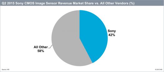
Sony has been wildly successful in the growing, but also highly competitive image sensor market. This has been true going back to the 1980s, when Sony CCDs powered devices such as camcorders and corporate security cameras. Sony was able to transition smoothly as the market moved to CMOS image sensors for camera phones and tablets. Today, it dominates the CMOS image sensor business, with Q2 2015 revenues of slightly over USD1 billion, good for over 42 percent of the worldwide market, nearly three times the revenue of its closest competitor, Samsung Electronics.
In the face of this market dominance of image sensors, the question arises for Sony: Why interfere with a good thing? The current Sony corporate structure seemed to be working well enough to ensure image sensor success. How will the new Sony Semiconductor Solutions benefit the image sensor business? The answer may be in simplifying a corporate structure so that Sony can react more rapidly.
If Sony has had a weakness in the image sensor market, it has been exploiting new markets and getting new sensors to market quickly. A recent example is the release of CMOS sensors with 1.0-micron pixels, the next step in CMOS phone sensor design. Both OmniVision and Samsung have already announced 1.0-micron models, while Sony has not. Also, Sony has been slow to new, emerging applications such as automotive cameras. It has just entered the automotive space in 2015, while competitors such as ON Semiconductor (through its acquisition of Aptina) have dominated the market for years.
Sony has stated that one of the purposes of its semiconductor spin out strategy is the "to more rapidly adapt to their respective changing market environments and generate sustained growth." And the old Sony structure was somewhat difficult for the image sensor business. In addition to its size being a barrier to quick decisions, the old system included Sony Semiconductor Corporation for image sensor manufacturing and Sony LSI Design for design operations. Under the new structure, both units will be combined under Sony Semiconductor Solutions.
At first glance, it seems unlikely that Sony could improve its already dominant position in the image sensor market. However, the spin out to a new organization that allows Sony to respond more quickly to market changes, and speed time-to-market for new designs, may have precisely that result.


