+44 (0)24 7671 8970
More publications     •     Advertise with us     •     Contact us
 
News Article

Wafer ID Reader developed by IOSS and HTT

News

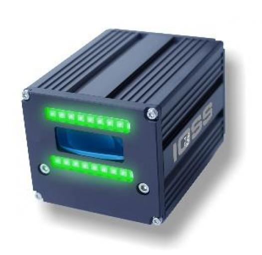
The IOSS WID110 Wafer ID Reader was developed by IOSS and HTT especially to meet the high demands of the semiconductor industry.

It easily decodes OCR, Barcode, DataMatrix and QR-Code markings on any kind of wafer regardless of the wafer material.

Thanks to the unique IOSS patented optical system and RGB (red-green-blue) illumination, the IOSS WID110 Wafer ID reader can image any ID mark. The fully automatic intuitive bright and multiple dark field illuminations offer a huge number of variations for the user. Up to 15 light modes as well as an auto-adjustment function are included in this state of the art wafer ID reader system. These self-contained systems with a compact design achieve highest read rates and counts with customer proven reliability.

The flexible recipe handling offers additional options to fulfil special application requirements. Per trigger the IOSS WID110 Wafer ID Reader can adjust up to 10.000 different settings. Two readers can operate at the same time on a single reader interface to read front- and backside (master/slave functionality) using one trigger.

IOSS is located in Radolfzell next to Lake Bodensee in Germany and is also the manufacturer of the reader system.

HTT owns exclusive sales right for the WID110 Wafer ID Reader worldwide.

Purdue, imec, Indiana announce partnership
Resilinc partners with SEMI on supply chain resilience
NIO and NXP collaborate on 4D imaging radar deployment
Panasonic Industry digitally transforms with Blue Yonder
Global semiconductor sales decrease 8.7%
MIT engineers “grow” atomically thin transistors on top of computer chips
Keysight joins TSMC Open Innovation Platform 3DFabric Alliance
Leti Innovation Days to explore microelectronics’ transformational role
Quantum expansion
indie launches 'breakthrough' 120 GHz radar transceiver
Wafer fab equipment - facing uncertain times?
Renesas expands focus on India
Neuralink selects Takano Wafer Particle Measurement System
Micron reveals committee members
Avoiding unscheduled downtime in with Preventive Vacuum Service
NFC chip market size to surpass US$ 7.6 billion
Fujifilm breaks ground on new €30 million European expansion
Fraunhofer IIS/EAS selects Achronix embedded FPGAs
Siemens announces certifications for TSMC’s latest processes
EU Chips Act triggers further €7.4bn investment
ASE recognised for excellence by Texas Instruments
Atomera signs license agreement with STMicroelectronics
Gartner forecasts worldwide semiconductor revenue to decline 11% in 2023
CHIPS for America outlines vision for the National Semiconductor Technology Center
TSMC showcases new technology developments
Alphawave Semi showcases 3nm connectivity solutions
Greene Tweed to open new facility in Korea
Infineon enables next-generation automotive E/E architectures
Global AFM market to reach $861.5 million
Cepton expands proprietary chipset
Semtech adds two industry veterans to board of directors
Specialty gas expansion
×
Search the news archive

To close this popup you can press escape or click the close icon.
Logo
×
Logo
×
Register - Step 1

You may choose to subscribe to the Silicon Semiconductor Magazine, the Silicon Semiconductor Newsletter, or both. You may also request additional information if required, before submitting your application.


Please subscribe me to:


You chose the industry type of "Other"

Please enter the industry that you work in: