
Tezzaron Announces World's First Eight-Layer Active Wafer Stack
Tezzaron Semiconductor and their manufacturing subsidiary, Novati Technologies, have announced the world's first eight-layer 3D IC wafer stack containing active logic. The transistor and interconnect densities per cubic mm are far higher than achievable with 2D 14nm silicon fabrication, promising to accelerate high-performance computing and put Moore's Law back on track, potentially saving the industry billions of dollars. "Passive wafer stacks have been built in labs, but this is the first time wafers containing actual circuitry have been stacked eight high," says Bob Patti, founder and CTO of Tezzaron. "And they were stacked in a manufacturing facility, not a lab."
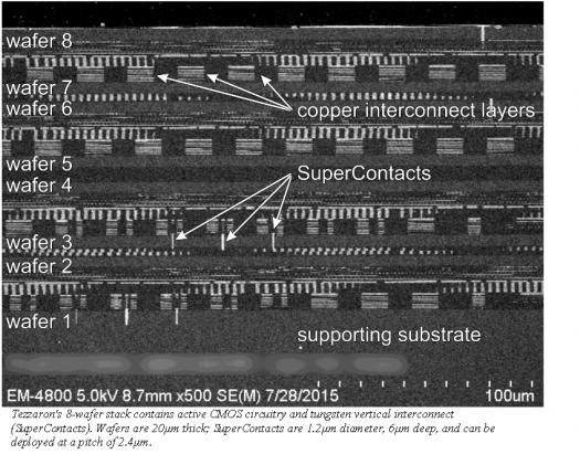
The stack represents the densest 3D IC ever reported. Each wafer has 10 layers of copper interconnect supporting high performance CMOS logic "“a total of 80 layers of interconnect and 8 layers of transistors in a finished stack as thin as a single conventional die.
The wafers were bonded with DBI technology, invented by Ziptronix and now available from Tessera. Paul Enquist, VP at Tessera, congratulated Tezzaron/Novati, the first licensee of the technology for 3D memory applications: "This milestone clearly demonstrates the enabling capability of DBI® to achieve transistor scale
3D interconnect pitch with Tezzaron's SuperContact technology, which we believe has an iterative capability beyond eight layers."Tezzaron's IC design and fabrication technology creates true 3D integrated circuits. There are no wire bonds, copper pillars, bumps, or underfill between the layers. It is not a 3D packaging technology that stacks 2D dies into 3D assemblies. Instead, the wafers are bonded directly, wafer-to-wafer, producing devices that can be finished to the same thickness as conventional 2D dies. The result is excellent electrical, thermal, and mechanical performance.
Each wafer in the finished stack is only 20μm thick. This allows vertical interconnect through the stack to be extremely dense and electrically unobtrusive, capable of carrying very small and fast signals. Tezzaron uses 1.2μm diameter tungsten SuperContacts rather than conventional copper TSVs. SuperContacts can be used at a 2.4μm pitch with no required keep-out zones near active transistors, so densities can exceed 170 thousand vertical connections per square mm. This is 350 times denser than state- of "“ the - art copper TSV vertical interconnect.
"The extravagant interconnect is very significant," says Bob Patti. "We can completely reconfigure any circuit and integrate it tightly in all three dimensions for superior performance at one - tenth the power." "This is another great milestone for the world - class nanomanufacturing at Novati," said David Anderson, President and CEO of Novati. "The 3D technologies being installed by Tezzaron are available to all of our customers. Our successes with Tezzaron's cutting - edge products are inspiring our 3D customers to push forward even faster.


