
Yield Engineering Systems Receives Multi-Million Dollar Orders from Taiwan
Yield Engineering Systems, Inc. (YES), a Silicon Valley Semiconductor Equipment Manufacturer, has begun large volume shipments of Wafer Thermal Curing Ovens to a major IC Fab in Taiwan. YES continues the ramp-up in manufacturing into the second quarter of 2016. Installations of the 4 FOUP, 300/200mm Polymer Thermal Process Equipment began in 2015.
Wafer Level Packaging (WLP) using Fan-Out Technology is a preferred platform for achieving low-cost, low profile packaging solutions. Smart phones, tablets and other mobile technologies require cost-effective, high density interconnects. Yield Engineering Systems (YES) thermal processes support the 3DIC, Fan-out Wafer Level Packaging and other Wafer Level Packing processes which have highly critical thermal steps.
Yield Engineering Systems PB Series Thermal Cure ovens are ideal for polyimides, PBO's and BCB cures. The ovens feature highly controlled temperatures, lowest O2 counts, excellent particle performance and controlled temperature ramping. The YES-PB Cure Oven allows flexible processing to accommodate a wide variety of substrates and materials.
In order to best support customers in Taiwan and China, YES is currently collaborating with Fortrend Engineering (Hsinchu), integrating YES-PB Vacuum Cure Ovens with Fortrend Equipment Front End Module (EFEM). By coordinating the transport of through-silicon via (TSV) and wafer level package (WLP) wafers to YES' back-end ovens, provides thermal curing with accurate temperature control in a fully-automated package for chip manufacturers. The combined front end integration with YES cure ovens has created an environment that is essential to the success of the wafer-level packaging industry.
YES-PB Series high temperature vacuum cure ovens are designed for today's most advanced polymer processing applications, which include:
- Polyimide/PBO cure
- BCB bake
- Low temp polymers cure
- Copper anneal
- Low-K dielectric cure
- Copper oxide removal
- Aluminum anneal
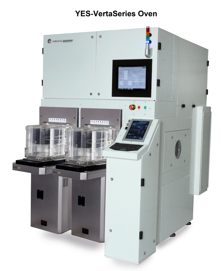
YES offers worldwide Fully-Automated YES-VertaCure High Temperature (controlled from ambient to 450°C) Vacuum Cure Ovens that are FOUP to FOUP, SMIF to SMIF or cassette to cassette for 200 and 300 mm wafers. YES also designs and manufactures the YES-450PB Series manual load High Temperature Vacuum Cure Ovens for all wafer sizes up to 300mm wafers.
YES-PB Series Cure Ovens offer these solutions:
1.Complete imidization with no trapped solvents
2.Optimized film adhesion performance
3.Removal of residual solvents and extraneous gases
4.Removal of photosensitive components
5.Simple design "“ easy to change polymer filter to protect plumbing and vacuum pumps
6.Controlled vacuum/hot Nitrogen purges
7.Low cost of ownership
"Yield Engineering Systems is excited by this significant ramp up in equipment sales," said Bill Moffat, founder and CEO of YES, "Our quality process equipment, and partnership with Fortrend in Taiwan, ensued in this multi-million dollar order. This has pushed us in the forefront of the Taiwan industry. Our high quality vacuum cure ovens increase good die yield which saves our customer considerable money in time and material. We support the success of our customers, who are always #1."


