
Nanostructured metal coatings let the light through for electrical devices
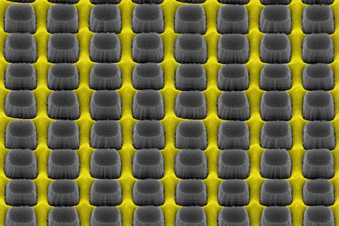
An array of nanopillars etched by thin layer of grate-patterned metal creates a nonreflective yet conductive surface that could improve electronic device performance. Image courtesy of Daniel Wasserman
Light and electricity dance a complicated tango in devices like LEDs, solar cells and sensors. A new anti-reflection coating developed by engineers at the University of Illinois at Urbana Champaign, in collaboration with researchers at the University of Massachusetts at Lowell, lets light through without hampering the flow of electricity, a step that could increase efficiency in such devices.
The coating is a specially engraved, nanostructured thin film that allows more light through than a flat surface, yet also provides electrical access to the underlying material "“ a crucial combination for optoelectronics, devices that convert electricity to light or vice versa. The researchers, led by U. of I. electrical and computer engineering professor Daniel Wasserman, published their findings in the journal Advanced Materials.
"The ability to improve both electrical and optical access to a material is an important step towards higher-efficiency optoelectronic devices," said Wasserman, a member of the Micro and Nano Technology Laboratory at Illinois.
At the interface between two materials, such as a semiconductor and air, some light is always reflected, Wasserman said. This limits the efficiency of optoelectronic devices. If light is emitted in a semiconductor, some fraction of this light will never escape the semiconductor material.
Alternatively, for a sensor or solar cell, some fraction of light will never make it to the detector to be collected and turned into an electrical signal. Researchers use a model called Fresnel's equations to describe the reflection and transmission at the interface between two materials.
"It has been long known that structuring the surface of a material can increase light transmission," said study co-author Viktor Podolskiy, a professor at the University of Massachusetts at Lowell.
"Among such structures, one of the more interesting is similar to structures found in nature, and is referred to as a "˜moth-eye' pattern: tiny nanopillars which can "˜beat' the Fresnel equations at certain wavelengths and angles."
Although such patterned surfaces aid in light transmission, they hinder electrical transmission, creating a barrier to the underlying electrical material.
"In most cases, the addition of a conducting material to the surface results in absorption and reflection, both of which will degrade device performance," Wasserman said.
The Illinois and Massachusetts team used a patented method of metal-assisted chemical etching, MacEtch, developed at Illinois by Xiuling Li, U. of I. professor of electrical and computer engineering and co-author of the new paper. The researchers used MacEtch to engrave a patterned metal film into a semiconductor to create an array of tiny nanopillars rising above the metal film. The combination of these "moth-eye" nanopillars and the metal film created a partially coated material that outperformed the untreated semiconductor.
"The nanopillars enhance the optical transmission while the metal film offers electrical contact. Remarkably, we can improve our optical transmission and electrical access simultaneously," said Runyu Liu, a graduate researcher at Illinois and a co-lead author of the work along with Illinois graduate researcher Xiang Zhao and Massachusetts graduate researcher Christopher Roberts.
The researchers demonstrated that their technique, which results in metal covering roughly half of the surface, can transmit about 90 percent of light to or from the surface. For comparison, the bare, unpatterned surface with no metal can only transmit 70 percent of the light and has no electrical contact.
The researchers also demonstrated their ability to tune the material's optical properties by adjusting the metal film's dimensions and how deeply it etches into the semiconductor.
"We are looking to integrate these nanostructured films with optoelectronic devices to demonstrate that we can simultaneously improve both the optical and electronic properties of devices operating at wavelengths from the visible all the way to the far infrared," Wasserman said.
The National Science Foundation and Lam Research supported this work.


