+44 (0)24 7671 8970
More publications     •     Advertise with us     •     Contact us
 
News Article

Okmetic introduce enhanced SOI wafer


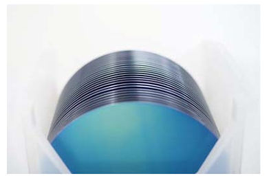
Okmetic has introduced an Enhanced SOI wafer (E-SOI) into its SOI product family (Silicon-On-Insulator).

The company believes that because of its new level of layer thickness uniformity and unprecedented properties E-SOI is an ideal platform for applications such as HV BCD devices, silicon photonics and high-precision silicon-based MEMS sensors.

"The device layer thickness of E-SOI is freely adjustable between 1.0 μm and >100 μm and the thickness tolerance independent of target thickness is as low as +/-0.1 μm. With the wide selection of silicon starting materials from Okmetic's in -house crystal growth, and similar flexibility in wafer customization as Okmetic BSOI wafers, the E-SOI technology provides an ideal wafer solution to both semiconductor and sensor applications", describes Senior Development Manager, Technology Jari Mäkinen, who was the leader of the development project.

Okmetic's SOI (Silicon-On-Insulator) wafers are manufactured by bonding technology. Two silicon wafers are bonded together, having an insulating oxide between. In a typical application sensing elements and possible IC devices are built on the active layer. Buried oxide is an effective etch-stop, and can also act as a sacrificial layer.

Handle wafer is supporting the structure but it can also be utilized in sealing the structure or as part of the sensing element. In addition to E-SOI, Okmetic's SOI family includes Bonded SOI (BSOI) and Cavity SOI (C-SOI) wafers. 

"Okmetic's strategic focus is on high-performance wafers for the manufacture of sensors, discrete semiconductors and analog circuits. E-SOI complements Okmetic's wide product selection perfectly and provides our customers an ideal platform for the manufacture of high-end devices", concludes Anna-Riikka Vuorikari -Antikainen, Okmetic's Senior Vice President, Customers and Markets.

Purdue, imec, Indiana announce partnership
Resilinc partners with SEMI on supply chain resilience
NIO and NXP collaborate on 4D imaging radar deployment
Panasonic Industry digitally transforms with Blue Yonder
Global semiconductor sales decrease 8.7%
MIT engineers “grow” atomically thin transistors on top of computer chips
Keysight joins TSMC Open Innovation Platform 3DFabric Alliance
Leti Innovation Days to explore microelectronics’ transformational role
Quantum expansion
indie launches 'breakthrough' 120 GHz radar transceiver
Wafer fab equipment - facing uncertain times?
Renesas expands focus on India
Neuralink selects Takano Wafer Particle Measurement System
Micron reveals committee members
Avoiding unscheduled downtime in with Preventive Vacuum Service
NFC chip market size to surpass US$ 7.6 billion
Fujifilm breaks ground on new €30 million European expansion
Fraunhofer IIS/EAS selects Achronix embedded FPGAs
Siemens announces certifications for TSMC’s latest processes
EU Chips Act triggers further €7.4bn investment
ASE recognised for excellence by Texas Instruments
Atomera signs license agreement with STMicroelectronics
Gartner forecasts worldwide semiconductor revenue to decline 11% in 2023
CHIPS for America outlines vision for the National Semiconductor Technology Center
TSMC showcases new technology developments
Alphawave Semi showcases 3nm connectivity solutions
Greene Tweed to open new facility in Korea
Infineon enables next-generation automotive E/E architectures
Global AFM market to reach $861.5 million
Cepton expands proprietary chipset
Semtech adds two industry veterans to board of directors
Specialty gas expansion
×
Search the news archive

To close this popup you can press escape or click the close icon.
Logo
×
Logo
×
Register - Step 1

You may choose to subscribe to the Silicon Semiconductor Magazine, the Silicon Semiconductor Newsletter, or both. You may also request additional information if required, before submitting your application.


Please subscribe me to:


You chose the industry type of "Other"

Please enter the industry that you work in: