
Plating Tools That Can Do More Than Plate
ClassOne Technology, manufacturer of electroplating systems, has announced their new Plating-Plus capability, which allows additional processes to be integrated into a single plating tool. This can optimize utilization of the ≤200mm Solstice plating equipment and give substantial net cost savings as well as process enhancements.
"A lot of our customers, especially those with low to moderate production levels, are seeing significant benefits in incorporating additional processes into our Solstice plating tool," said Win Carpenter, ClassOne's V.P. of International Sales. "With Plating-Plus many users can eliminate the need to purchase additional downstream equipment "” and that eliminates the costs of adding floor space, operators, training, spare parts, etc. Our customers can maximize the use of a single Solstice and streamline their process flow. They can gain the benefits of single-wafer processing with reduced queue times and less excess capacity. The result is a more efficient solution with better capacity matching and lower overall costs."
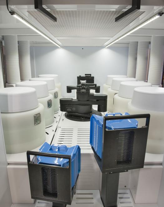
"Plating-Plus is made possible because of the unique flexibility we designed into our Solstice plating tools right from the start," said Kevin Witt, President of ClassOne Technology. "The Solstice S8 provides eight modular chamber positions that can be used for different processes "” all within one standard, highly reliable platform. Users can get the special functionality they want simply by ordering their new Solstice with a specific configuration of chambers."
Three new advanced chambers
To date, ClassOne has introduced three new modular Plating-Plus processing chambers that can be installed on Solstice plating tools. These are high-performance, high-efficiency chambers that enable High-Pressure Metal Lift-Off, Resist Strip, and UBM (Under Bump Metallization) Etch. The new ClassOne High-Pressure Metal Lift-Off chamber is designed for high-efficiency metal removal without redeposition. The Resist Strip chamber is an advanced spray module that handles solvents safely and can run a single stripping process across a range of different resists. The UBM Etch Chamber incorporates an intelligent optical end-point detection technology that controls etching precisely and consistently to avoid undercut.
The new Plating-Plus capabilities are making Solstice a highly productive tool for advanced packaging, MEMS, LEDs, opto-electronics and more. The multi-processing system is well suited to a range of needs, from patterned plating to RDL, from flip-chip/bump/wafer level packaging to applications that require through-resist plating, resist removal and etching of seed layers.
Going forward, ClassOne plans to add more new Plating-Plus chambers to cover additional processes. Pricing for each of these chambers is designed to be significantly less than the costs of adding a new stand-alone tool.
The Solstice electroplating line serves many cost-sensitive emerging markets such as MEMS, Sensors, LEDs, RF and others that use 200mm and smaller wafers. Solstice tools are available in three different models for production and development and can electroplate many different metals and alloys, either on transparent or opaque substrates. Solstice systems are priced at less than half of what similarly configured plating systems from the larger manufacturers would cost "” which is why Solstice has been described as "Advanced Plating for the Rest of Us."


