
EV GROUP expands high-vacuum wafer bonding capabilities for MEMS
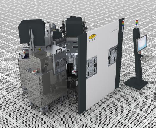
EV Group (EVG), a supplier of wafer bonding and lithography equipment for the MEMS, nanotechnology and semiconductor markets, has introduced new capabilities on the EVG ComBond automated high-vacuum wafer bonding platform specifically designed to support high-volume manufacturing (HVM) of advanced MEMS devices. These capabilities include a new vacuum bond alignment module that provides sub-micron face-to-face alignment accuracy essential for wafer-level MEMS packaging, and a new bake module that performs critical process steps to achieve outstanding bond quality and performance of encapsulated MEMS devices.
The addition of these two new modules"”coupled with existing capabilities on the highly configurable EVG ComBond platform such as room-temperature covalent bonding of engineered substrates"”enables customers to meet the wafer bonding requirements for both current and emerging types of MEMS devices. Examples include gyroscopes, microbolometers, and advanced sensors for autonomous cars, virtual reality headsets and other applications.
"When EV Group introduced the EVG ComBond platform, we set a new standard in high-vacuum wafer bonding by building the product around a modular, highly customizable cluster design concept. This has enabled us to continually expand the capabilities of the platform over time, with applications ranging from advanced engineered substrates, power devices and solar cells to high-performance logic and "˜Beyond CMOS' devices," stated Paul Lindner, executive technology director, EV Group. "With the addition of new vacuum alignment and bake modules, those wafer bonding capabilities have been expanded yet again to address the volume manufacturing needs for high-end MEMS devices."
Challenges of Scaling MEMS Wafer Bonding into Production
Many MEMS devices have extremely small moving parts, which must be protected from the external environment. Wafer-level capping can seal a wafer's worth of MEMS devices in one operation, and these capped devices can then be packaged into much simpler and lower-cost packages. Metal-based aligned wafer bonding is the preferred approach to MEMS wafer bonding, but is challenging to implement due to the high process temperatures involved as well as the presence of oxides that form on the bonding metal layers. As MEMS die and feature sizes decrease, achieving tighter wafer alignment accuracy also becomes increasingly important.
At the same time, vacuum encapsulation is increasingly needed for certain MEMS devices in order to reduce power consumption caused by parasitic drag, reduce convection heat transfer, or prevent oxide corrosion. Maintaining the required vacuum level for the entire wafer bonding process has been a key challenge for ramping these devices into high-volume production.
"ƒ


