
Scientists Reveal Inner Workings of Atomically Thin Transistors
With an eye to the next generation of tech gadgetry, a team of physicists at The University of Texas at Austin has had the first-ever glimpse into what happens inside an atomically thin semiconductor device. In doing so, they discovered that an essential function for computing may be possible within a space so small that it's effectively one-dimensional.
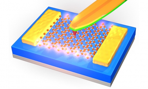
In a paper published in July in the Proceedings of the National Academy of Sciences, the researchers describe seeing the detailed inner workings of a new type of transistor that is two-dimensional.
Transistors act as the building blocks for computer chips, sending the electrons on and off switches required for computer processing. Future tech innovations will require finding a way to fit more transistors on computer chips, so experts have begun exploring new semiconducting materials including one called molybdenum disulfide (MoS2). Unlike today's silicon-based devices, transistors made from the new material allow for on-off signaling on a single flat plane.
Keji Lai, an assistant professor of physics, and a team found that with this new material, the conductive signaling happens much differently than with silicon, in a way that could promote future energy savings in devices. Think of silicon transistors as light bulbs: The whole device is either turned on or off at once. With 2-D transistors, by contrast, Lai and the team found that electric currents move in a more phased way, beginning first at the edges before appearing in the interior. Lai says this suggests the same current could be sent with less power and in an even tinier space, using a one-dimensional edge instead of the two-dimensional plane.
"In physics, edge states often carry a lot of interesting phenomenon, and here, they are the first to turn on. In the future, if we can engineer this material very carefully, then these edges can carry the full current," Lai says. "We don't really need the entire thing, because the interior is useless. Just having the edges running to get a current working would substantially reduce the power loss."
Researchers have been working to get a view into what happens inside a 2-D transistor for years to better understand both the potential and the limitations of the new materials. Getting 2-D transistors ready for commercial devices, such as paper-thin computers and cellphones, is expected to take several more years. Lai says scientists need more information about what interferes with performance in devices made from the new materials.
"These transistors are perfectly two-dimensional," Lai says. "That means they don't have some of the defects that occur in a silicon device. On the other hand, that doesn't mean the new material is perfect."
Lai and his team used a microscope that he invented and that points microwaves at the 2-D device. Using a tip only 100 nanometres wide, the microwave microscope allowed the scientists to see conductivity changes inside the transistor. Besides seeing the currents' motion, the scientists found thread-like defects in the middle of the transistors. Lai says this suggests the new material will need to be made cleaner to function optimally.
"If we could make the material clean enough, the edges will be carrying even more current, and the interior won't have as many defects," Lai says.
The paper's other authors are postdoctoral researchers Di Wu and Xiao Li; research scientist Lan Luan, and graduate students Xiaoyu Wu and Zhaodong Chu, and professor Qian Niu in UT Austin's Department of Physics; and graduate student Wei Li, former graduate student Maruthi N. Yogeesh, postdoctoral researcher Rudresh Ghosh, and associate professor Deji Akinwande of UT Austin's Department of Electrical and Computer Engineering.
Earlier this year, both Lai and Akinwande won Presidential Early Career Awards for Scientists and Engineers, the U.S. government's highest honor for early-stage scientists and engineers.
The research was supported by the U.S. Department of Energy, as well as the Welch Foundation, the Office of Naval Research and the National Science Foundation.


