
Beneq strengthens its position in high-volume industrial ALD
Beneq, a supplier of ALD equipment and thin film coating services, has announced two new thin film equipment solutions for industrial customers that require high capacity and low process cost in advanced ALD applications. The new products are set to revolutionize the standards of coating speed in the ALD industry.
Beneq R11 is the latest addition to Beneq's portfolio of large-throughput spatial ALD solutions for industrial use. It provides an optimal solution for high performance ALD on wafers in industrial applications, such as optical coatings, insulators and barriers. It is the ideal choice of equipment when speed, cost, low process temperature and the highest possible film quality are the driving factors.
With Beneq R11, it is for the first time possible to use PEALD (Plasma Enhanced ALD) processes in high volume manufacturing. The system lends itself to barrier, insulation and anti-corrosion applications for MEMS, LED, OLED, photovoltaics, high power semiconductors, sensors and many other components.
The equipment is suitable for up to 200 mm wafers and other round or rectangular substrates. The plasma enhanced rotary ALD process of Beneq R11 is ideal for thick ALD films, in the micrometer thickness range. Beneq R11 can also be equipped with standard wafer automation.
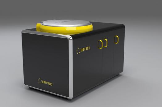
Beneq T2S is the newest member of Beneq's wafer-based production equipment portfolio. It offers a unique combination of high capacity batch processing and standard cassette-to-cassette automation. The Beneq T2S is specifically engineered to match the semiconductor requirements, including the SEMI S2 safety requirements and low particle counts.
Beneq T2S is perfectly suited for high volume manufacturing in various wafer-based applications, including MEMS, LED, OLED, ink-jet print heads and more. The thermal batch ALD process of Beneq T2S is ideal for oxide and nitride processes used for dielectric, conductor, barrier and passivation purposes.
The equipment is designed for wafers up to 200 mm in diameter and can process 25 wafers per run in face-down or face-up orientation.
New products officially unveiled in ALD2016 in Dublin, Ireland
Both new products, Beneq R11 and Beneq T2S, will be introduced officially for the first time at ALD2016 "“ the 16th International Conference on Atomic Layer Deposition, which will be held at the Convention Centre Dublin, Ireland, 24-27, July 2016. Beneq is a platinum sponsor of the event.
Says Tommi Vainio, Vice President, Thin Film Equipment, at Beneq: "High capacity industrial ALD solutions are an important and expanding part of our product portfolio. Our commitment to revolutionize the coating speed standards in the ALD industry is clearly demonstrated in the new ALD equipment we are launching in Dublin. From now on with Beneq, the unit for ALD area is m2 instead of mm2."


