Exploiting the new wave of Semiconductors: AI, trust & information overload

Robert McKenzie, VP of Silicon Sector at global software services company, Mobica navigates the semiconductor revolution and identifies opportunities for growth.
The global semiconductor industry is experiencing huge growth and predicted to become a trillion dollar industry by 2030. That growth is being accompanied by an ongoing rediscovery of application approaches and step changes in design and development. It is not an understatement to say that we are seeing momentous changes happening at an unprecedented pace. In this article we take a look at what’s driving those changes, their adoption and the technology underlying this momentous change.
The scale of change
A keynote at Embedded World conference, March 2023, provided the following eye popping statistics about the level of growth in Internet of Things (IoT) business and installations:
£ By 2030, the IoT could enable $5.5 trillion to $12.6 trillion in value globally
£ In 2023 11.5bn connected devices will ship, bringing the installed base to 40bn
units - 1.5bn home automation, 0.75bn inventory and
asset tracking, 600m for lighting, 300m
health and fitness
Thanks to the rapid adoption of
AI, embedded solutions and the IoT, there is a new wave of chips coming along
that can serve a broader range of applications. They can do so because of the
increased capability to support security, safety, identity and privacy, all
areas where the new architecture and semiconductor chip features add value.
Originally computers were designed for a particular purpose, for example, breaking cryptographic ciphers. The arrival of the first commercially available general purpose computer, the Ferranti Mark 1, led to general purpose applications for government, business and scientific challenges. But there was still an opportunity for ‘application specific integrated chips’ (ASICS). Companies such as LSI Logic played a significant role in changing the semiconductor market during the 1980s and 90s, with their ASICS for calculators etc.
Building on the foundations
laid over the past 50 years
Today’s industry builds on
previous inventions to deliver a wide range of architectures and technologies
that deliver the new applications. As well as the general purpose ‘central
processing units’ (CPUs), those technologies include:
£ ASICS for handling, amongst other things, compression, encryption and with features like VRAN boost in Intel XEON based SmartNICS accelerating networking needs.
£ FPGAs - fully programmable gate arrays - enabling feature updates on the semiconductor itself, making them as upgradeable as a software package
£ GPUs - graphics processing units - accelerating graphics processing by enabling single instructions to operate in parallel on multiple data
£ xPUs - the processing unit designed for a particular application
The ‘system on chip’ (SOC) approach brings together semiconductor designs to deal with I/O, power management, telecoms, including the iterations of mobile protocols 3-5g, WAN and Bluetooth.
We should mention the concept of the xPU: this is a catch-all for the ‘processing unit’, designed for a particular application e.g. most SOCs now include an NPU, or neural processing unit, designed for efficiently calculating the mathematics of neural networks, which feature in new products from Intel, Apple and Qualcomm. A further example is the VPU, or ‘visual process unit’, used in cameras, and designed for image processing.
Scaling up: trends and new
developments
As well as being able to design
all the systems on one chip, standardisation around ‘chiplets’ will increase
the possibility and market for new semiconductor development.
The UCIe specification for the ‘Universal Chiplet Interconnect Express’ is focussed on building an open ecosystem of chiplets for on-package innovations. This market will take a decade to develop, but is part of the new wave of semiconductor innovation.
Before moving onto AI, trust and information overload, it’s worth providing two more examples of scale. At the data centre end, Nvidia’s GPU Technology Conference in 2022, Stephen Jones ran through the phenomenal increase in performance that has occurred at the high-end of silicon technology.
The A100 GPU, or Ampere architecture, used in the data-centres, runs at 9.7 TFLOP/s double precision performance. To put this in perspective, the world’s leading supercomputer in 2001 was the Lawrence Livermore National Laboratory in the USA’s ASCI White, had 7.9 TFLOPS/s. So the A100 chip has more than the equivalent performance.
At the recent GTC, Jensen Huang - Nvidia’s CEO - announced its new Blackwell architecture to be released in 2024. Whilst double precision (FP16) performance figures weren’t presented, the new chip does deliver 20k TFLOPS at FP4, or 1000x increase over the past 8 years.
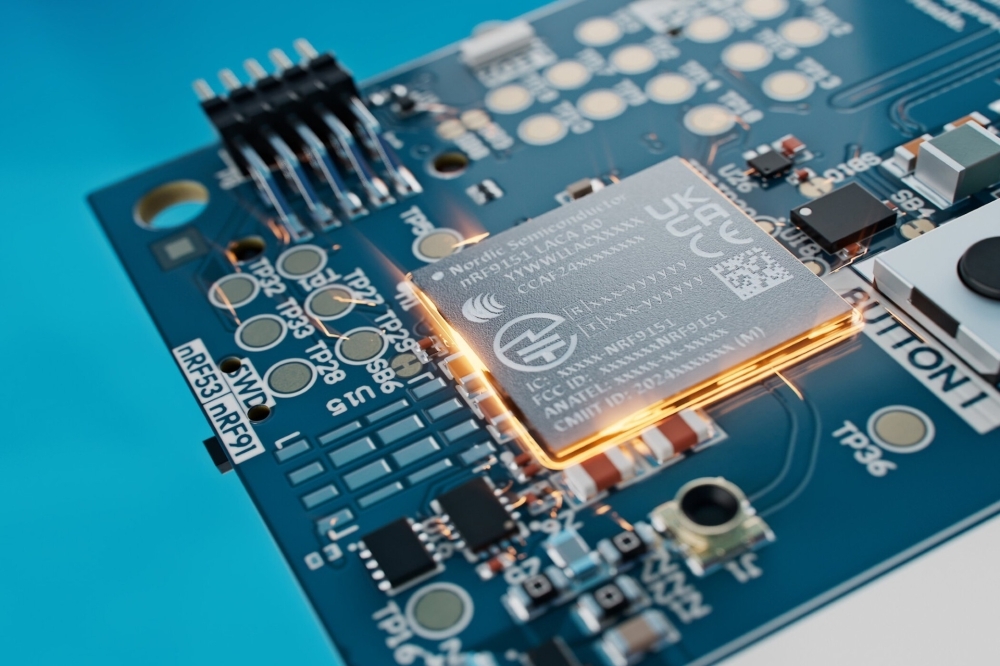
At the edge, the microcontroller (MCU) is becoming increasingly sophisticated and able to deliver more. Traditionally it has a few components such as RAM, ROM, and programmable I/O ports primarily designed to control and drive other electronic equipment. MCUs are designed to be embedded, often in a highly restrictive environment. They usually consume very little power, may run relatively slow, and typically execute individual task-specific programs. But now they are increasingly including features to ensure security and provide AI services.
TinyML is one movement that is enabling machine learning on these tiny devices. According to the TinyML foundation, it is broadly defined as a fast growing field of machine learning technologies and applications including hardware, algorithms and software capable of performing on-device sensor data analytics at extremely low power, typically in the mW range and below, which enables a variety of always-on uses for battery operated devices.
The NXP MCX N Advanced Series Microcontrollers, includes intelligent peripherals and on-chip accelerators. To balance performance and power efficiency, they incorporate NXP’s eIQ Neutron neural processing unit (NPU) specifically for machine learning applications.
Similar devices are being produced by Infineon, STMicro, Sony, Espressif, often combining off the shelf IP CPU cores licensed from ARM and then adding these new features in order to support new applications. Whereas the latest data centre chips and boards cost tens of thousands of dollars, microcontrollers can be bought in quantity for under fifteen dollars - or less.
Further new innovations coming down the line will increase the performance and reduce the power consumption even further. A good example of this is being developed by EnchargeAI. They are designing a hybrid of analogue and digital chip technology due to ship at the end of 2024. Benchmarks demonstrate a 150 TOPS/W, which is 20x current market leader in power usage efficiency.
Inference: use cases and
applications
Initial use cases for the
EnchargeAI product will be in inference, not for training the Deep Neural Nets
(DNN) and Large Language Models that Nvidia and newer entrants such as
Tenstorrent and Cerebras are aiming at. The inference work will use these trained
models for natural language processing and image recognition support. The
product is likely to become integrated in SOCs for the phone, or battery
powered devices. Currently, security systems are often wired in because the
components won’t operate for multi-year periods on batteries. These new
technologies bring the promise that they will not only be able to operate for
long periods of time, but that they will also be able to make decisions based
on better training.
At the moment, standard commercial or domestic security systems will recognise intruders, capture the image and, if armed, inform the owner. With new features at an improved price point, it’s a short step to having the system recognise that it’s you, or someone else who lives or works at the premises, and disarm and open the door.
For the first time, the ability to get inferencing and then decision making right at the edge is becoming a reality. Perhaps more significantly, it is also becoming economically viable.
So much so that a number of companies such as Google’s advanced projects and Levi and Nike have been championing the use of wearable technology. For Nike, this is in the sporting field, where its value in assessing fitness and performance is married with the far more important need to understand the long-term health of athletes, especially in contact sports.
Mobica has worked on SOLI for gesture recognition (radar) and Jacquard (gyro) for motion. Jacquard technology used by Levi’s and Nike, Soli technology features in the Pixel phone.
Semiconductors form the bedrock for these applications but need the software and firmware above it in order to put an ecosystem in place that makes it a usable solution.
The two fundamental technological areas of artificial intelligence (AI) and trust, which is more typically referred to as security, have driven the demand for new semiconductor design and performance. The software and firmware part of the journey is also vital.
Connecting the hardware to
the software
The capability of connecting the
hardware to the software is at the core of Mobica - a Cognizant company -
services. When a device needs a driver, whether it be GPU or Ethernet adapter,
Mobica is often asked to assist and we cover all other aspects of connecting
the hardware by developing and optimising systems software and firmware.
Our customers included industry leaders such as BMW, Jaguar Land Rover, Cariad in the automotive industry and ARM, Imagination Technologies as well as Samsung in the semiconductor industry.
The customers of these customers are demanding smarter products, which now means using AI and products they can trust, which means better security technology.
The new wave of chips -
privacy, security and trust
This new wave of chips supports
trust in new products and services, but
includes well understood cryptographic theory as features in the chip set or
SOC. The algorithm was initially devised by mathematician Clifford Cocks who,
in the early 1970s, while working at the United Kingdom Government Communications
Headquarters (GCHQ), developed public key cryptography (PKC). It was developed
into a solution known as public key encryption (PKE), by Rivest, Shamir and
Adleman (RSA) who established a company to commercialise it.
This algorithm and digital certificates infrastructure has been widely used since the 1990’s - but it has been implemented at the network, (the IP layer) to deliver ‘virtual private networks’ (VPNs) with IPSec protocol and at the Transport layer, via the TLS implementation, to deliver security to web browsers, text messages and email for example. The problem is that neither of these prevents interception or ‘man in the middle’ attacks at the physical media level - that is the processor.
Consequently semiconductor industry participants have developed frameworks and IP to ensure that customer information and data can remain private, not only when ‘at rest’ i.e in a storage medium, or when ‘in flight’ i.e. over communication protocols such as HTTP, but now when ‘in use’. The expression ‘secure, at rest, in flight and in use’ has become commonplace over the last 3-5 years.
Two companies that have introduced semiconductor technology to support this are Intel and ARM. Intel is most famously associated with the PC and data centre, whereas ARM licences technology to companies such as Apple, Qualcomm and Samsung and, between these two ecosystems, the cloud to edge security is covered.
Intel delivered the Intel Trust Authority, offering a unified independent assessment of its Trusted Platform Module. TPM came from the Trusted Computing consortium and provides circuitry to implement PKI down to the processor level in both the PC and data centre. The Trust Authority provides a framework for independent attestation that nothing has touched, read, or in any way interfered with your data.
The key point is that the TA services will give users confidence that confidential information placed in the cloud remains secret, even from those that operate the cloud. There is nothing that they can do, at the container, hypervisor or OS level that gives them the privileges to access this. This is vitally important for many industries e.g. banking, pharmaceutical, for its drug research data chemical industries, for product recipes.
ARM provides its Platform Security Architecture (PSA) as a common industry framework for IoT devices. PSA helps developers define a consistent level of security by providing principles and deliverables, including threat models, architecture specifications and open source firmware.
For its Cortex A architecture, the heart of most mobile phone SOCs, it has created Trust Zone, which is commonly used to run trusted boot and trusted OS to create a Trusted Execution Environment (TEE). Typical use cases include the protection of authentication mechanisms, cryptography, mobile device management, payment, key material, and digital rights management (DRM).
These two frameworks add the semiconductor integrity to well understood trust algorithms, providing the integrity required for customer trust of the product. Naturally, even though these foundations are in place, it requires excellent and experienced software and firmware engineering to implement an error free solution. Mobica works with chip manufacturers and smart product manufacturers to ensure that the implementation includes all valid specifications and verifies that the specifications are implemented accurately.
To the consumer, they can have confidence that these products and services will prevent unauthorised access to property or theft of vehicles. If used for monitoring services - and if the provider transfers sole access and data to the consumer - then the same technology can be used to prevent ‘big brother’ scenarios, whether from government or organisations.
The future functions of AI
PC
The AI features in the new
semiconductor solutions work in tandem with trust features to combat
information overload. The vast majority of work activity today requires
handling large amounts of information and data.
Recently at Mobile World Congress (MWC) in Barcelona, a partner discussion posited a few examples of where AI assistants either help, or may help, reduce overload. The first example was for office productivity where the new AI PC - which was being promoted - would feature applications that could summarise and prioritise emails and the coming week’s meetings, in conversation with the PC. This might be possible, but there is a lot of software engineering and LLM training and application development to be done before this would work faster and more accurately than doing it yourself.
As the diversity of document and file types and stores proliferate, this capability will be much needed - particularly thanks to phones, drives (Apple, Gdrive, Onedrive) mail (Gmail, Outlook, Thunderbird, Apple), messaging apps (Slack, WhatsApp, Messenger) and social media (Snapchat, Facebook, Instagram, TikTok).
This is particularly the case since the AI PC is taking the workload off the CPU, resulting in a more responsive and power efficient PC. For example, tests show that blurring the background for video conferencing (an AI task) takes up to 20% of CPU cycles. This goes down to 1% with the AI NPU offload and gives a 38% power saving when tested with ZOOM. Further examples included translating sign-language to english in real-time which was not possible with earlier PC generations but is now a possibility, using CPU, GPU and NPU in the AI PC to deliver this.
Microsoft has co-opted the term ‘Co-pilot’ for embedding AI technology into OS’s and applications. It’s a good term, better than ‘digital twin’ as it confers the notion of assistance. As Mobica is a software and firmware solution provider, benefits from assistance in writing both are appreciated, but it’s not a panacea, even for programming, where logic and algorithms are documented in Open Source repositories such as GitHub and GitLab.
The best illustration of the journey still to be taken was presented by Fireship - a popular technology YouTube channel. It’s worth looking at ‘Devin’ - a product from Cognition AI labs - which accesses a terminal, browser, coder editor like a SW engineer and is designed to work like an SW engineering expert. It iterates, through from requirement, to code fragments similar to the issue and generates code, runs it, tests it and more, until the requirement is met.
As a product, it is comparable to AutoGPT, where LLM is also the base technology, but Devin gets the ability to perform actions and react to the feedback from those actions.
They demonstrated the product using the “SW Engineering Benchmark”, which is closer to real SW engineering challenges, than what is commonly used for demonstrating other ‘co-pilot’ type products.
The benchmark provides an evaluation framework including 2,294 software engineering problems drawn from real GitHub issues and corresponding pull requests across 12 popular Python repositories. Given a codebase along with a description of an issue to be resolved, a language model is tasked with editing the codebase to address the issue.
The table below shows the results:
Whilst 13.85% is a step change compared to previous LLM products benchmark results, it is not the end of software and firmware engineering as a career. In fact the need for experienced engineers is likely to continue to grow.
The ongoing importance of
software engineering
The new performant semiconductor
products provide the foundation for these new solutions, both in the cloud
(large scale) and at the edge (small scale), but engineering the complete stack
requires skilled software engineering services.
It is imperative that we continue to train and develop engineers that understand the performance parameters, strengths and characteristics of new and developing software, whether that’s AI technologies (LLMs, SLMs, DNN RNNs), cryptographic, compression or performance accelerators, which is something Mobica, and its parent Cognizant delivers.


